
Chapter 4
PARASITIC EXTRACTION AND PERFORMANCE ESTIMATION
FROM PHYSICAL STRUCTURE
![[previous]](../left.gif)
![[Table of Contents]](../toc.gif)
![[next]](../right.gif)
In this chapter, we will investigate some of the physical factors which determine and ultimately limit the performance of digital VLSI circuits. The switching characteristics of digital integrated circuits essentially dictate the overall operating speed of digital systems. The dynamic performance requirements of a digital system are usually among the most important design specifications that must be met by the circuit designer. Therefore, the switching speed of the circuits must be estimated and optimized very early in the design phase.
The classical approach for determining the switching speed of a digital block is based on the assumption that the loads are mainly capacitive and lumped. Relatively simple delay models exist for logic gates with purely capacitive load at the output node, hence, the dynamic behavior of the circuit can be estimated easily once the load is determined. The conventional delay estimation approaches seek to classify three main components of the gate load, all of which are assumed to be purely capacitive, as: (1) internal parasitic capacitances of the transistors, (2) interconnect (line) capacitances, and (3) input capacitances of the fan-out gates. Of these three components, the load conditions imposed by the interconnection lines present serious problems.
![[Zoom]](Figure-4.1.gif)
Figure 4.1 shows a simple situation where an inverter is driving three other inverters, linked over interconnection lines of different length and geometry. If the total load of each interconnection line can be approximated by a lumped capacitance, then the total load seen by the primary inverter is simply the sum of all capacitive components described above. The switching characteristics of the inverter are then described by the charge/discharge time of the load capacitance, as seen in Fig. 4.2. The expected output voltage waveform of the inverter is given in Fig. 4.3, where the propagation delay time is the primary measure of switching speed. It can be shown very easily that the signal propagation delay under these conditions is linearly proportional to the load capacitance.
In most cases, however, the load conditions imposed by the interconnection line are far from being simple. The line, itself a three-dimensional structure in metal and/or polysilicon, usually has a non-negligible resistance in addition to its capacitance. The length/width ratio of the wire usually dictates that the parameters are distributed, making the interconnect a true transmission line. Also, an interconnect is very rarely “alone”, i.e., isolated from other influences. In real conditions, the interconnection line is in very close proximity to a number of other lines, either on the same level or on different levels. The capacitive/inductive coupling and the signal interference between neighboring lines should also be taken into consideration for an accurate estimation of delay.
![[Zoom]](Figure-4.2.gif)
![[Zoom]](Figure-4.3.gif)
![[Top of Document]](../top.gif)
Consider the following situation where an inverter is driving two other inverters, over long interconnection lines. In general, if the time of flight across the interconnection line (as determined by the speed of light) is shorter than the signal rise/fall times, then the wire can be modeled as a capacitive load, or as a lumped or distributed RC network. If the interconnection lines are sufficiently long and the rise times of the signal waveforms are comparable to the time of flight across the line, then the inductance also becomes important, and the interconnection lines must be modeled as transmission lines. Taking into consideration the RLCG (resistance, inductance, capacitance, and conductance) parasitics (as seen in Fig. 4.4), the signal transmission across the wire becomes a very complicated matter, compared to the relatively simplistic lumped- load case. Note that the signal integrity can be significantly degraded especially when the output impedance of the driver is significantly lower than the characteristic impedance of the transmission line.
![[Zoom]](Figure-4.4.gif)
The transmission-line effects have not been a serious concern in CMOS VLSI until recently, since the gate delay originating from purely or mostly capacitive load components dominated the line delay in most cases. But as the fabrication technologies move to finer (sub- micron) design rules, the intrinsic gate delay components tend to decrease dramatically. By contrast, the overall chip size does not decrease - designers just put more functionality on the same sized chip. A 100 mm2 chip has been a standard large chip for almost a decade. The factors which determine the chip size are mainly driven by the packaging technology, manufacturing equipment, and the yield. Since the chip size and the worst-case line length on a chip remain unchanged, the importance of interconnect delay increases in sub-micron technologies. In addition, as the widths of metal lines shrink, the transmission line effects and signal coupling between neighboring lines become even more pronounced.
This fact is illustrated in Fig. 4.5, where typical intrinsic gate delay and interconnect delay are plotted qualitatively, for different technologies. It can be seen that for sub-micron technologies, the interconnect delay starts to dominate the gate delay. In order to deal with the implications and to optimize a system for speed, the designers must have reliable and efficient means of (1) estimating the interconnect parasitics in a large chip, and (2) simulating the time- domain effects. Yet we will see that neither of these tasks is simple - interconnect parasitic extraction and accurate simulation of line effects are two of the most difficult problems in physical design of VLSI circuits today.
![[Zoom]](Figure-4.5.gif)
Once we establish the fact that the interconnection delay becomes a dominant factor in CMOS VLSI, the next question is: how many of the interconnections in a large chip may cause serious problems in terms of delay. The hierarchical structure of most VLSI designs offers some insight on this question. In a chip consisting of several functional modules, each module contains a relatively large number of local connections between its functional blocks, logic gates, and transistors. Since these intra-module connections are usually made over short distances, their influence on speed can be simulated easily with conventional models. Yet there are also a fair amount of longer connections between the modules on a chip, the so-called inter-module connections. It is usually these inter-module connections which should be scrutinized in the early design phases for possible timing problems. Figure 4.6 shows the typical statistical distribution of wire lengths on a chip, normalized for the chip diagonal length. The distribution plot clearly exhibits two distinct peaks, one for the relatively shorter intra-module connections, and the other for the longer inter-module connections. Also note that a small number of interconnections may be very long, typically longer than the chip diagonal length. These lines are usually required for global signal bus connections, and for clock distribution networks. Although their numbers are relatively small, these long interconnections are obviously the most problematic ones.
![[Zoom]](Figure-4.6.gif)
To summarize the message of this section, we state that : (1) interconnection delay is becoming the dominating factor which determines the dynamic performance of large-scale systems, and (2) interconnect parasitics are difficult to model and to simulate. In the following sections, we will concentrate on various aspects of on-chip parasitics, and we will mainly consider capacitive and resistive components.
The first component of capacitive parasitics we will examine is the MOSFET capacitances. These parasitic components are mainly responsible for the intrinsic delay of logic gates, and they can be modeled with fairly high accuracy for gate delay estimation. The extraction of transistor parasitics from physical structure (mask layout) is also fairly straightforward.
The parasitic capacitances associated with a MOSFET are shown in Fig. 4.7 as lumped elements between the device terminals. Based on their physical origins, the parasitic device capacitances can be classified into two major groups: (1) oxide-related capacitances and (2) junction capacitances. The gate-oxide-related capacitances are Cgd (gate-to-drain capacitance), Cgs (gate-to-source capacitance), and Cgb (gate-to-substrate capacitance). Notice that in reality, the gate-to-channel capacitance is distributed and voltage dependent. Consequently, all of the oxide-related capacitances described here change with the bias conditions of the transistor. Figure 4.8 shows qualitatively the oxide-related capacitances during cut-off, linear-mode operation and saturation of the MOSFET. The simplified variation of the three capacitances with gate-to-source bias voltage is shown in Fig. 4.9.
![[Zoom]](Figure-4.7.gif)
![[Zoom]](Figure-4.8.gif)
Note that the total gate oxide capacitance is mainly determined by the parallel-plate capacitance between the polysilicon gate and the underlying structures. Hence, the magnitude of the oxide-related capacitances is very closely related to (1) the gate oxide thickness, and (2) the area of the MOSFET gate. Obviously, the total gate capacitance decreases with decreasing device dimensions (W and L), yet it increases with decreasing gate oxide thickness. In sub-micron technologies, the horizontal dimensions (which dictate the gate area) are usually scaled down more easily than the horizontal dimensions, such as the gate oxide thickness. Consequently, MOSFET transistors fabricated using sub-micron technologies have, in general, smaller gate capacitances.
![[Zoom]](Figure-4.9.gif)
Now we consider the voltage-dependent source-to-substrate and drain-to-substrate capacitances, Csb and Cdb. Both of these capacitances are due to the depletion charge surrounding the respective source or drain regions of the transistor, which are embedded in the substrate. Figure 4.10 shows the simplified geometry of an n-type diffusion region within the p-type substrate. Here, the diffusion region has been approximated by a rectangular box, which consists of five planar pn-junctions. The total junction capacitance is a function of the junction area (sum of all planar junction areas), the doping densities, and the applied terminal voltages. Accurate methods for estimating the junction capacitances based on these data are readily available in the literature, therefore, a detailed discussion of capacitance calculations will not be presented here.
One important aspect of parasitic device junction capacitances is that the amount of capacitance is a linear function of the junction area. Consequently, the size of the drain or the source diffusion area dictates the amount of parasitic capacitance. In sub-micron technologies, where the overall dimensions of the individual devices are scaled down, the parasitic junction capacitances also decrease significantly.
It was already mentioned that the MOSFET parasitic capacitances are mainly responsible for the intrinsic delay of logic gates. We have seen that both the oxide-related parasitic capacitances and the junction capacitances tend to decrease with shrinking device dimensions, hence, the relative significance of intrinsic gate delay diminishes in sub-micron technologies.
![[Zoom]](Figure-4.10.gif)
In a typical VLSI chip, the parasitic interconnect capacitances are among the most difficult parameters to estimate accurately. Each interconnection line (wire) is a three dimensional structure in metal and/or polysilicon, with significant variations of shape, thickness, and vertical distance from the ground plane (substrate). Also, each interconnect line is typically surrounded by a number of other lines, either on the same level or on different levels. Figure 4.11 shows a possible, realistic situation where interconnections on three different levels run in close proximity of each other. The accurate estimation of the parasitic capacitances of these wires with respect to the ground plane, as well as with respect to each other, is obviously a complicated task.
![[Zoom]](Figure-4.11.gif)
Unfortunately for the VLSI designers, most of the conventional computer-aided VLSI design tools have a relatively limited capability of interconnect parasitic estimation. This is true even for the design tools regularly used for sub-micron VLSI design, where interconnect parasitics were shown to be very dominant. The designer should therefore be aware of the physical problem and try to incorporate this knowledge early in the design phase, when the initial floorplanning of the chip is done.
First, consider the section of a single interconnect which is shown in Fig. 4.12. It is assumed that this wire segment has a length of (l) in the current direction, a width of (w) and a thickness of (t). Moreover, we assume that the interconnect segment runs parallel to the chip surface and is separated from the ground plane by a dielectric (oxide) layer of height (h). Now, the correct estimation of the parasitic capacitance with respect to ground is an important issue. Using the basic geometry given in Fig. 4.12, one can calculate the parallel-plate capacitance Cpp of the interconnect segment. However, in interconnect lines where the wire thickness (t) is comparable in magnitude to the ground-plane distance (h), fringing electric fields significantly increase the total parasitic capacitance (Fig. 4.13).
![[Zoom]](Figure-4.12.gif)
![[Zoom]](Figure-4.13.gif)
![[Zoom]](Figure-4.14.gif)
A set of simple formulas developed by Yuan and Trick in the early 1980’s can be used to estimate the capacitance of the interconnect structures in which fringing fields complicate the parasitic capacitance calculation. The following two cases are considered for two different ranges of line width (w).
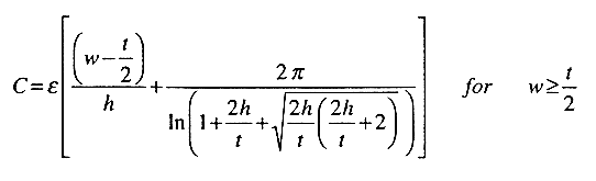 (4.1)
(4.1)
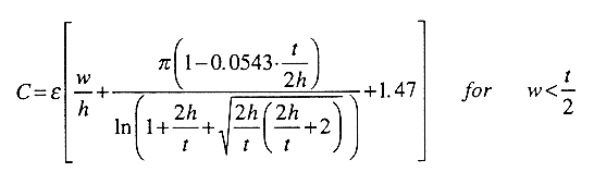 (4.2)
(4.2)
These formulas permit the accurate approximation of the parasitic capacitance values to within 10% error, even for very small values of (t/h). Figure 4.15 shows a different view of the line capacitance as a function of (w/h) and (t/h). The linear dash-dotted line in this plot represents the corresponding parallel-plate capacitance, and the other two curves represent the actual capacitance, taking into account the fringing-field effects.
![[Zoom]](Figure-4.15.gif)
Now consider the more realistic case where the interconnection line is not “alone” but is coupled with other lines running in parallel. In this case, the total parasitic capacitance of the line is not only increased by the fringing-field effects, but also by the capacitive coupling between the lines. Figure 4.16 shows the capacitance of a line which is coupled with two other lines on both sides, separated by the minimum design rule. Especially if both of the neighboring lines are biased at ground potential, the total parasitic capacitance of the interconnect running in the middle (with respect to the ground plane) can be more than 20 times as large as the simple parallel-plate capacitance. Note that the capacitive coupling between neighboring lines is increased when the thickness of the wire is comparable to its width.
![[Zoom]](Figure-4.16.gif)
Figure 4.17 shows the cross-section view of a double-metal CMOS structure, where the individual parasitic capacitances between the layers are also indicated. The cross-section does not show a MOSFET, but just a portion of a diffusion region over which some metal lines may pass. The inter-layer capacitances between the metal-2 and metal-1, metal-1 and polysilicon, and metal-2 and polysilicon are labeled as Cm2m1, Cm1p and Cm2p, respectively. The other parasitic capacitance components are defined with respect to the substrate. If the metal line passes over an active region, the oxide thickness underneath is smaller (because of the active area window), and consequently, the capacitance is larger. These special cases are labeled as Cm1a and Cm2a. Otherwise, the thick field oxide layer results in a smaller capacitance value.
![[Zoom]](Figure-4.17.gif)
The vertical thickness values of the different layers in a typical 0.8 micron CMOS technology are given below as an example.
Field oxide thickness         	0.52 	um
Gate oxide thickness          	16.0	nm
Poly 1 thickness              	0.35 	um	 (minimum width 0.8 um)
Poly-metal oxide thickness    	0.65 	um
Metal 1 thickness             	0.60 	um	 (minimum width 1.4 um)
Via oxide thickness           	1.00 	um
Metal 2 thickness             	1.00 	um	 (minimum width 1.6 um)
n+ junction depth             	0.40 	um
p+ junction depth             	0.40 	um
n-well junction depth         	3.50 	um
The list below contains the capacitance values between various layers, also for a typical 0.8 micron CMOS technology.
Poly over field oxide		(area)		0.066		fF/um2
Poly over field oxide		(perimeter)	0.046		fF/um

Metal-1 over field oxide	(area)		0.030		fF/um2
Metal-1 over field oxide	(perimeter)	0.044		fF/um

Metal-2 over field oxide	(area)		0.016		fF/um2
Metal-2 over field oxide	(perimeter)	0.042		fF/um

Metal-1 over poly		(area)		0.053		fF/um2
Metal-1 over poly		(perimeter)	0.051		fF/um

Metal-2 over poly		(area)		0.021		fF/um2
Metal-2 over poly		(perimeter)	0.045		fF/um

Metal-2 over metal-1		(area)		0.035		fF/um2
Metal-2 over metal-1		(perimeter)	0.051		fF/um
For the estimation of interconnect capacitances in a complicated three-dimensional structure, the exact geometry must be taken into account for every portion of the wire. Yet this requires an unacceptable amount of computation in a large circuit, even if simple formulas are applied for the calculation of capacitances. Usually, chip manufacturers supply the area capacitance (parallel-plate cap) and the perimeter capacitance (fringing-field cap) figures for each layer, which are backed up by measurement of capacitance test structures. These figures can be used to extract the parasitic capacitances from the mask layout. It is often prudent to include test structures on chip that enable the designer to independently calibrate a process to a set of design tools. In some cases where the entire chip performance is influenced by the parasitic capacitance of a specific line, accurate 3-D simulation is the only reliable solution.
The parasitic resistance of a metal or polysilicon line can also have a profound influence on the signal propagation delay over that line. The resistance of a line depends on the type of material used (polysilicon, aluminum, gold, ...), the dimensions of the line and finally, the number and locations of the contacts on that line. Consider again the interconnection line shown in Fig. 4.12. The total resistance in the indicated current direction can be found as
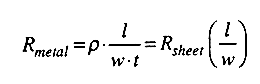 (4.2)
(4.2)
where the greek letter ro represents the characteristic resistivity of the interconnect material, and Rsheet represents the sheet resistivity of the line, in (ohm/square). For a typical polysilicon layer, the sheet resistivity is between 20-40 ohm/square, whereas the sheet resistivity of silicide is about 2- 4 ohm/square. Using the formula given above, we can estimate the total parasitic resistance of a wire segment based on its geometry. Typical metal-poly and metal-diffusion contact resistance values are between 20-30 ohms, while typical via resistance is about 0.3 ohms.
In most short-distance aluminum and silicide interconnects, the amount of parasitic wire resistance is usually negligible. On the other hand, the effects of the parasitic resistance must be taken into account for longer wire segments. As a first-order approximation in simulations, the total lumped resistance may be assumed to be connected in series with the total lumped capacitance of the wire. A much better approximation of the influence of distributed parasitic resistance can be obtained by using an RC-ladder network model to represent the interconnect segment (Fig. 4.18). Here, the interconnect segment is divided into smaller, identical sectors, and each sector is represented by an RC-cell. Typically, the number of these RC-cells (i.e., the resolution of the RC model) determines the accuracy of the simulation results. On the other hand, simulation time restrictions usually limit the resolution of this distributed line model.
![[Zoom]](Figure-4.18.gif)
This chapter edited by Y. Leblebici