
![[previous]](left.gif)
![[Table of Contents]](toc.gif)
![[next]](right.gif)
The purpose of this chapter is to give an overview of the different components used in the design of arithmetic operators. The following parts will not exhaustively go through all these components. However, the algorithms used, some mathematical concepts, the architectures, the implementations at the block, transistor or even mask level will be presented. This chapter will start by the presentation of various notation systems. Those are important because they influence the architectures, the size and the performance of the arithmetic components. The well known and used principle of generation and propagation will be explained and basic implementation at transistor level will be given as examples. The basic full adder cell (FA) will be shown as a brick used in the construction of various systems. After that, the problem of building large adders will lead to the presentation of enhancement techniques. Multioperand adders are of particular interest when building special CPU's and especially multipliers. That is why, certain algorithms will be introduced to give a better idea of the building of multipliers. After the show of the classical approaches, a logarithmic multiplier and the multiplication and addition in the Galois Fields will be briefly introduced. Muller [Mull92] and Cavanagh [Cava83] constitute two reference books on the matter.
![[Top of Document]](top.gif)
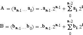
where ai=0 or 1 for i in [0, n-1]. This vector can represent positive integer values V = A in the range 0 to 2n-1, where:
The above representation can be extended to include fractions. An example follows. The string of binary digits 1101.11 can be interpreted to represent the quantity :
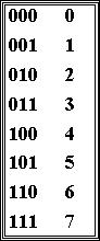
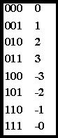
The following Table 1 shows the 3-bit vector representing the decimal expression to the right.
In this representation, the high-order bit indicates the sign of the integer (0 for positive, 1 for negative). A positive number has a range of 0 to 2n-1-1, and a negative number has a range of 0 to -(2n-1-1). The representation of a positive number is :
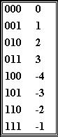
In this representation, the high-order bit also indicates the sign of the integer (0 for positive, 1 for negative). A positive number has a range of 0 to 2n-1-1, and a negative number has a range of 0 to -(2n-1-1). The representation of a positive number is :
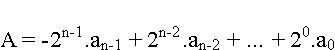
In this notation system (radix 2), the value of A is represented such as:
in which all the digits of the set are positively weighted. It is also possible to have a digit set in which both positive- and negative-weighted digits are allowed [Aviz61] [Taka87], such as:
 (6)
(6) is
called the ceiling of .
is
called the ceiling of .
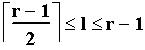
For any number x , the ceiling of x is the smallest integer not less than x. The floor of x , is the largest integer not greater than x. Since the integer l bigger or equal than 1 and r bigger or equal than 2, then the maximum magnitude of l will be
Thus for r=2, the digit set is:
For r=4, the digit set is
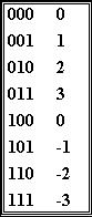
For example, for n=4 and r=2, the number A=-5 has four representation as shown below on Table 5.
| 23 | 22 | 21 | 20 | |
| A= | 0 | -1 | 0 | -1 |
| A= | 0 | -1 | -1 | 1 |
| A= | -1 | 0 | 1 | 1 |
| A= | -1 | 1 | 0 | -1 |
This multirepresentation makes redundant number systems difficult to use for certain arithmetic operations. Also, since each signed digit may require more than one bit to represent the digit, this may increase both the storage and the width of the storage bus.
However, redundant number systems have an advantage for the addition which is that is possible to eliminate the problem of the propagation of the carry bit. This operation can be done in a constant time independent of the length of the data word. The conversion from binary to binary redundant is usually a duplication or juxtaposition of bits and it does not cost anything. On the contrary, the opposite conversion means an addition and the propagation of the carry bit cannot be removed.
Let us consider the example where r=2 and l=1. In this system the three used digits are -1, 0, +1.
The representation of 1 is 10, because 1-0=1.
The representation of -1 is 01, because 0-1=-1.
One representation of 0 is 00, because 0-0=0.
One representation of 0 is 11, because 1-1=0.
The addition of 7 and 5 give 12 in decimal. The same is equivalent in a binary non redundant system to 111 + 101:
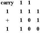
We note that a carry bit has to be added to the next digits when making the operation "by hand". In the redundant system the same operation absorbs the carry bit which is never propagated to the next order digits:
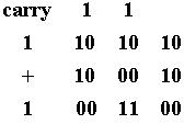
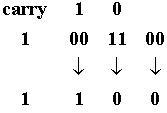
The result 1001100 has now to be converted to the binary non redundant system. To achieve that, each couple of bits has to be added together. The eventual carry has to be propagated to the next order bits:
This means that when ai=bi, it is possible to add the bits greater than the ith, before the carry information ci+1 has arrived. The time required to perform the addition will be proportional to the length of the longest chain i,i+1, i+2, i+p so that ak not equal to bk for k in [i,i+p].
It has been shown [BGNe46] that the average value of this longest chain
is proportional to the logarithm of the number of bits used to represent
A and B. By using this principle of generation and propagation it is possible
to design an adder with an average delay o(log n). However, this type of
adder is usable only on asynchronous systems [Mull82]. Today the complexity
of the systems is so high that asynchronous timing of the operations is
rarely implemented. That is why the problem is rather to minimize the maximum
delay rather than the average delay.
Generation:
All adders which use this principle calculate in a first stage.
![[Zoom]](Figure-6.1.gif)
This implementation can be very performant (20 transistors) depending on the way the XOR function is built. The carry propagation of the carry is controlled by the output of the XOR gate. The generation of the carry is directly made by the function at the bottom. When both input signals are 1, then the inverse output carry is 0.
In the schematic of Figure 6.1, the carry passes through a complete transmission gate. If the carry path is precharged to VDD, the transmission gate is then reduced to a simple NMOS transistor. In the same way the PMOS transistors of the carry generation is removed. One gets a Manchester cell.
![[Zoom]](Figure-6.2.gif)
The Manchester cell is very fast, but a large set of such cascaded cells would be slow. This is due to the distributed RC effect and the body effect making the propagation time grow with the square of the number of cells. Practically, an inverter is added every four cells, like in Figure 6.3.
![[Zoom]](Figure-6.3.gif)
The adder cell receives two operands ai and bi, and an incoming carry
ci. It computes the sum and the outgoing carry ci+1.
ci+1 = ai . bi + ai . ci
+ ci . bi = ai . bi +
(ai + bi ). ci ci+1 = pi
. ci + gi
![[Zoom]](Figure-6.4.gif)
where
These equation can be directly translated into two N and P nets of transistors leading to the following schematics. The main disadvantage of this implementation is that there is no regularity in the nets.
![[Zoom]](Figure-6.5.gif)
The dual form of each equation described previously can be written in the same manner as the normal form:
In the same way :
![[Zoom]](Figure-6.6.gif)
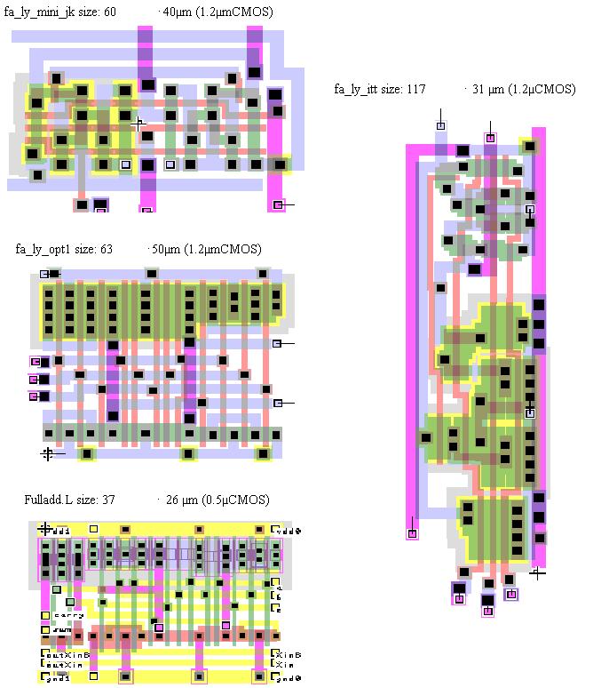
The following Figure 6.7 shows different physical layouts in different
technologies. The size, the technology and the performance of each cell
is summarized in the next Table 6.
| Name of cell | Number of Tr. | Size (µm2) | Technology | Worst Case Delay (ns) (Typical Conditions) |
| fa_ly_mini_jk | 24 | 2400 | 1.2 µ | 20 |
| fa_ly_op1 | 24 | 3150 | 1.2 µ | 5 |
| Fulladd.L | 28 | 962 | 0.5 µ | 1.5 |
| fa_ly_itt | 24 | 3627 | 1.2 µ | 10 |
![[Zoom]](Figure-6.8.gif)
Generally, the size of an adder is determined according to the type of operations required, to the precision or to the time allowed to perform the operation. Since the operands have a fixed size, if becomes important to determine whether or not there is a detected overflow
Overflow: An overflow can be detected in two ways. First an overflow has occurred when the sign of the sum does not agree with the signs of the operands and the sign s of the operands are the same. In an n-bit adder, overflow can be defined as:
Secondly, if the carry out of the high order numeric (magnitude) position of the sum and the carry out of the sign position of the sum agree, the sum is satisfactory; if they disagree, an overflow has occurred. Thus,
A parallel adder adds two operands, including the sign bits. An overflow from the magnitude part will tend to change the sign of the sum. So that an erroneous sign will be produced. The following Table 7 summarizes the overflow detection
| an-1 | bn-1 | sn-1 | cn-1 | cn-2 | Overflow |
| 0 | 0 | 0 | 0 | 0 | 0 |
| 0 | 0 | 1 | 0 | 1 | 1 |
| 1 | 1 | 0 | 1 | 0 | 1 |
| 1 | 1 | 1 | 1 | 1 | 0 |
Coming back to the acceleration of the computation, two major techniques are used: speed-up techniques (Carry Skip and Carry Select), anticipation techniques (Carry Look Ahead, Brent and Kung and C3i). Finally, a combination of these techniques can prove to be an optimum for large adders.
With a Ripple Carry Adder, if the input bits Ai and Bi are different for all position i, then the carry signal is propagated at all positions (thus never generated), and the addition is completed when the carry signal has propagated through the whole adder. In this case, the Ripple Carry Adder is as slow as it is large. Actually, Ripple Carry Adders are fast only for some configurations of the input words, where carry signals are generated at some positions.
Carry Skip Adders take advantage both of the generation or the propagation of the carry signal. They are divided into blocks, where a special circuit detects quickly if all the bits to be added are different (Pi = 1 in all the block). The signal produced by this circuit will be called block propagation signal. If the carry is propagated at all positions in the block, then the carry signal entering into the block can directly bypass it and so be transmitted through a multiplexer to the next block. As soon as the carry signal is transmitted to a block, it starts to propagate through the block, as if it had been generated at the beginning of the block. Figure 6.10 shows the structure of a 24-bits Carry Skip Adder, divided into 4 blocks.
![[Zoom]](Figure-6.9.gif)
![[Zoom]](Figure-6.10.gif)
To summarize, if in a block all Ai's?Bi's, then the carry signal skips over the block. If they are equal, a carry signal is generated inside the block and needs to complete the computation inside before to give the carry information to the next block.
OPTIMISATION TECHNIQUE WITH BLOCKS OF EQUAL SIZE
It becomes now obvious that there exist a trade-off between the speed and the size of the blocks. In this part we analyse the division of the adder into blocks of equal size. Let us denote k1 the time needed by the carry signal to propagate through an adder cell, and k2 the time it needs to skip over one block. Suppose the N-bit Carry Skip Adder is divided into M blocks, and each block contains P adder cells. The actual addition time of a Ripple Carry Adder depends on the configuration of the input words. The completion time may be small but it also may reach the worst case, when all adder cells propagate the carry signal. In the same way, we must evaluate the worst carry propagation time for the Carry Skip Adder. The worst case of carry propagation is depicted in Figure 6.11.
![[Zoom]](Figure-6.11.gif)
The configuration of the input words is such that a carry signal is generated at the beginning of the first block. Then this carry signal is propagated by all the succeeding adder cells but the last which generates another carry signal. In the first and the last block the block propagation signal is equal to 0, so the entering carry signal is not transmitted to the next block. Consequently, in the first block, the last adder cells must wait for the carry signal, which comes from the first cell of the first block. When going out of the first block, the carry signal is distributed to the 2nd, 3rd and last block, where it propagates. In these blocks, the carry signals propagate almost simultaneously (we must account for the multiplexer delays). Any other situation leads to a better case. Suppose for instance that the 2nd block does not propagate the carry signal (its block propagation signal is equal to zero), then it means that a carry signal is generated inside. This carry signal starts to propagate as soon as the input bits are settled. In other words, at the beginning of the addition, there exists two sources for the carry signals. The paths of these carry signals are shorter than the carry path of the worst case. Let us formalize that the total adder is made of N adder cells. It contains M blocks of P adder cells. The total of adder cells is then
The time T needed by the carry signal to propagate through P adder cells is
The time T' needed by the carry signal to skip through M adder blocks is
The problem to solve is to minimize the worst case delay which is:
So that the function to be minimized is:
The minimum is obtained for:
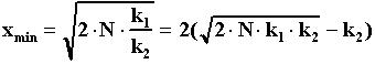 (30)
(30)OPTIMISATION TECHNIQUE WITH BLOCKS OF NON-EQUAL SIZE
Let us formalize the problem as a geometric problem. A square will represent the generic full adder cell. These cells will be grouped in P groups (in a column like manner).
L(i) is the value of the number of bits of one column.
L(1), L(2), ..., L(P) are the P adjacent columns. (see Figure 6.12)
![[Zoom]](Figure-6.12.gif)
If a carry signal is generated at the ith section, this carry skips j-i-1 sections and disappears at the end of the jth section. So the delay of propagation is:
By defining the constant a equal to:
 (32)
(32)one can position two straight lines defined by:
The constant a is equivalent to the slope dimension in the geometrical problem of the two two straight lines defined by equations (33) and (34). These straight lines are adjacent to the top of the columns and the maximum time can be expressed as a geometrical distance y equal to the y-value of the intersection of the two straight lines.
![[Zoom]](Figure-6.13.gif)
A possible implementation of a block is shown in Figure 6.14. In a precharged mode, the output of the four inverter-like structure is set to one. In the evaluation mode, the entire block is in action and the output will either receive c0 or the carry generated inside the comparator cells according to the values given to A and B. If there is no carry generation needed, c0 will be transmitted to the output. In the other case, one of the inversed pi's will switch the multiplexer to enable the other input.
![[Zoom]](Figure-6.14.gif)
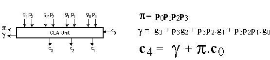
It can be seen that the group carries logic increases rapidly when more high- order groups are added to the total adder length. This complexity can be decreased, with a subsequent increase in the delay, by partitioning a long adder into sections, with four groups per section, similar to the CLA adder.
![[Zoom]](Figure-6.15.gif)
![[Zoom]](Figure-6.16.gif)
A possible implementation is shown on Figure 6.16, where it is possible to merge some redundant logic gates to achieve a lower complexity with a higher density.
Usually the size and complexity for a big adder using this equation is not affordable. That is why the equation is used in a modular way by making groups of carry (usually four bits). Such a unit generates then a group carry which give the right predicted information to the next block giving time to the sum units to perform their calculation.
Such unit can be implemented in various ways, according to the allowed level of abstraction. In a CMOS process, 17 transistors are able to guarantee the static function (Figure 6.18). However this design requires a careful sizing of the transistors put in series.
The same design is available with less transistors in a dynamic logic design. The sizing is still an important issue, but the number of transistors is reduced (Figure 6.19).
![[Zoom]](Figure-6.18.gif)
![[Zoom]](Figure-6.19.gif)
To build large adders the preceding blocks are cascaded according to Figure 6.20.
![[Zoom]](Figure-6.20.gif)
REFORMULATION OF THE CARRY CHAIN
Let an an-1 ... a1 and bn bn-1 ... b1 be n-bit binary numbers with sum sn+1 sn ... s1. The usual method for addition computes the sis by:
Where ++ means the sum modulo-2 and ci is the carry from bit position i. From the previous paragraph we can deduce that the cis are given by:
One can explain equation (44) saying that the carry ci is
either generated by ai and bi or propagated from
the previous carry ci-1. The whole idea is now to generate the
carrys in parallel so that the nth stage does not have to wait
for the n-1th carry bit to compute the global sum. To achieve
this goal an operator ![]() is defined.
is defined.
Let ![]() be defined as follows for any g, g', p and p' :
be defined as follows for any g, g', p and p' :
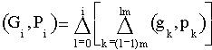
Lemma1: Let (Gi, Pi)
= (g1, p1) if i = 1 (48)
(gi, pi) ![]() (Gi-1, Pi-1) if i in [2, n] (49)
(Gi-1, Pi-1) if i in [2, n] (49)
Then ci = Gi for
i = 1, 2, ..., n.
Proof: The Lemma is proved by induction on i. Since c0 = 0, (44) above gives:
And from (44) we have : Gi = ci.
Lemma2: The operator ![]() is associative.
is associative.
Proof: For any (g3, p3), (g2,
p2), (g1, p1) we have:
[(g3, p3) ![]() (g2, p2)]
(g2, p2)] ![]() (g1, p1) = (g3+ p3 . g2,
p3 . p2)
(g1, p1) = (g3+ p3 . g2,
p3 . p2) ![]() (g1, p1)
(g1, p1)
= (g3+ p3 . g2+ , p3 .
p2 . p1) (55)
and,
(g3, p3) ![]() [(g2, p2)
[(g2, p2) ![]() (g1, p1)] = (g3, p3)
(g1, p1)] = (g3, p3) ![]() (g2 + p2 . g1, p2 . p1)
(g2 + p2 . g1, p2 . p1)
= (g3 + p3 . (g2 + p2 .
g1), p3 . p2 . p1) (56)
One can check that the expressions (55) and (56) are equal using the distributivity of . and +.
To compute the cis it is only necessary to compute all the (Gi, Pi)s but by Lemmas 1 and 2,
can be evaluated in any order from the given gis and pis. The motivation for introducing the operator Delta is to generate the carrys in parallel. The carrys will be generated in a block or carry chain block, and the sum will be obtained directly from all the carrys and pis since we use the fact that:
THE ADDER
Based on the previous reformulation of the carry computation Brent and Kung have proposed a scheme to add two n-bit numbers in a time proportional to log(n) and in area proportional to n.log(n), for n bigger or equal to 2. Figure 6.21 shows how the carrys are computed in parallel for 16-bit numbers.
![[Zoom]](Figure-6.21.gif)
Using this binary tree approach, only the cis where i=2k (k=0,1,...n) are computed. The missing cis have to be computed using another tree structure, but this time the root of the tree is inverted (see Figure 6.22).
In Figure 6.21 and Figure 6.22 the squares represent a ![]() cell which performs equation (47). Circles represent a duplication cell
where the inputs are separated into two distinct wires (see Figure 6.23).
cell which performs equation (47). Circles represent a duplication cell
where the inputs are separated into two distinct wires (see Figure 6.23).
When using this structure of two separate binary trees, the computation
of two 16-bit numbers is performed in T=9 stages of ![]() cells. During this time, all the carries are computed in a time necessary
to traverse two independent binary trees.
cells. During this time, all the carries are computed in a time necessary
to traverse two independent binary trees.
According to Burks, Goldstine and Von Neumann, the fastest way to add two operands is proportional to the logarithm of the number of bits. Brent and Kung have achieved such a result.
![[Zoom]](Figure-6.22.gif)
![[Zoom]](Figure-6.23.gif)
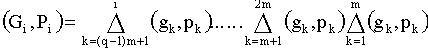
Let ai and bi be the digits of A and B, two n-bit numbers with i = 1, 2, ...,n. The carry's will be computed according to (59).
If we develop (59), we get:
and by introducing a parameter m less or equal than n so that it exists
q in IN | n = q.m, it is possible to obtain the couple (Gi,
Pi) by forming groups of m ![]() cells performing the intermediate operations detailed in (62) and (63).
cells performing the intermediate operations detailed in (62) and (63).
 (62)
(62) (63)
(63)This manner of computing the carries is strictly based on the fact that
the operator ![]() is associative. It shows also that the calculation is performed sequentially,
i.e. in a time proportional to the number of bits n. We will now illustrate
this analytical approach by giving a way to build an architectural layout
of this new algorithm. We will proceed to give a graphical method to place
the
is associative. It shows also that the calculation is performed sequentially,
i.e. in a time proportional to the number of bits n. We will now illustrate
this analytical approach by giving a way to build an architectural layout
of this new algorithm. We will proceed to give a graphical method to place
the ![]() cells
defined in the previous paragraph [Kowa92].
cells
defined in the previous paragraph [Kowa92].
THE GRAPHICAL CONSTRUCTIONM
![[Zoom]](Figure-6.24.gif)
At this point of the definition, two remarks have to be made about the definition of this algorithm. Both concern the m parameter used to defined the algorithm. Remark 1 specifies the case for m not equal to 2q (q in [0,1, ...] ) as Remark 2 deals with the case where m=n.
![[Zoom]](Figure-6.25.gif)
Remark 1: For m not a power of two, the algorithm is built the
same way up to the very last step. The only reported difference will concern
the delay which will be equal to the next nearest power of two. This means
that there is no special interest to build such versions of these adders.
The fan-out of certain cells is even increased to three, so that the electrical
behaviour will be degraded. Figure 6.25 illustrates the design of such
an adder based on m=6. The fan-out of the ![]() cell of bit 11 is three. The delay of this adder is equivalent to the delay
of an adder with a duplication with m=8.
cell of bit 11 is three. The delay of this adder is equivalent to the delay
of an adder with a duplication with m=8.
Remark 2: For m equal to the number of bits of the adder, the algorithm reaches the real theoretical limit demonstrated by Burks, Goldstine and Von Neumann. The logarithmic time is attained using one depth of a binary tree instead of two in the case of Brent and Kung. This particular case is illustrated in Figure 6.26. The definition of the algorithm is followed up to Step3. Once the reproduction of the binary tree is made m times to the right, the only thing to do is to remove the cells at the negative bit positions and the adder is finished. Mathematically, one can notice that this is the limit. We will discuss later whether it is the best way to build an adder using m=n.
![[Zoom]](Figure-6.26.gif)
COMPARISONS
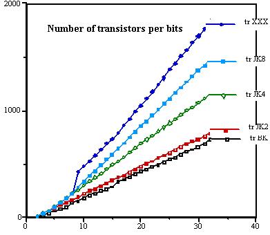
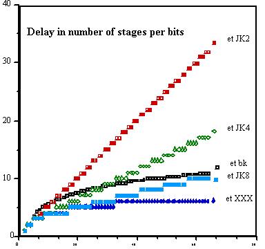
In this section, we develop a comparison between adders obtained using the new algorithm with different values of m. On the plots of Figure 6.27 through Figure 6.29, the suffixes JK2, JK4, and JK8 will denote different adders obtained for m equal two, four or eight. They are compared to the Brent and Kung implementation and to the theoretical limit which is obtained when m equals n, the number of bits.
The comparison between these architectures is done according to the
formalisation of a computational model described in [Kowa93]. We clearly
see that BKs algorithm performs the addition with a delay proportional
to the logarithm of the number of bits. JK2 performs the addition in a
linear time, just as JK4 or JK8. The parameter m influences the slope of
the delay. So that, the higher is m, the longer the delay stays under the
logarithmic delay of (BK). We see that when one wants to implement the
addition faster than (BK), there is a choice to make among different values
of m. The choice will depend on the size of the adder because it is evident
that a 24-bit JK2 adder (delay = 11 stages of ![]() cells) performs worse than BK (delay = 7 stages of
cells) performs worse than BK (delay = 7 stages of ![]() cells).
cells).
On the other hand JK8 (delay = 5 stages of ![]() cells) is very attractive. The delay is better than BK up to 57 bits. At
this point both delays are equal. Furthermore, even at equal delays (up
to 73 bits) our implementation performs better in terms of regularity,
modularity and ease to build. The strong advantage of this new algorithm
compared to BK is that for a size of the input word which is not a power-of-two,
the design of the cells is much easier. There is no partial binary tree
to build. The addition of a bit to the adder is the addition of a bit-slice.
This bit-slice is very compact and regular. Let us now consider the case
where m equals n (denoted by XXX on our figures). The delay of such an
adder is exactly one half of BK and it is the lowest bound we obtain. For
small adders (n < 16), the delay is very close to XXX. And it can be
demonstrated that the delays (always in term of stages) of JK2, JK4, JK8
are always at least equal to XXX.
cells) is very attractive. The delay is better than BK up to 57 bits. At
this point both delays are equal. Furthermore, even at equal delays (up
to 73 bits) our implementation performs better in terms of regularity,
modularity and ease to build. The strong advantage of this new algorithm
compared to BK is that for a size of the input word which is not a power-of-two,
the design of the cells is much easier. There is no partial binary tree
to build. The addition of a bit to the adder is the addition of a bit-slice.
This bit-slice is very compact and regular. Let us now consider the case
where m equals n (denoted by XXX on our figures). The delay of such an
adder is exactly one half of BK and it is the lowest bound we obtain. For
small adders (n < 16), the delay is very close to XXX. And it can be
demonstrated that the delays (always in term of stages) of JK2, JK4, JK8
are always at least equal to XXX.
This discussion took into account the two following characteristics of the computational model:
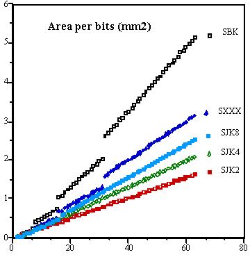
Here we could point out that the floorplan of BK could be optimised to become comparable to the one of XXX, but the cost of such an implementation would be very high because of the irregularity of the wirings and the interconnections. These considerations lead us to the following conclusion: to minimise the area of a new adder, m must be chosen low. This is contradictory with the previous conclusion. That is why a very wise choice of m will be necessary, and it will always depend on the targeted application. Finally, Figure 6.27 gives us the indications about the number of transistors used to implement our different versions of adders. These calculations are based on the dynamic logic family (TSPC: True Single Phase Clocking) described in [Kowa93]. When considering this graph, we see that BK and XXX are two limits of the family of our adders. BK uses the smallest number of transistors , whereas XXX uses up to five times more transistors. When m is highest, the number of transistors is highest.
Nevertheless, we see that the area is smaller than BK. A high density is an advantage, but an overhead in transistors can lead to higher power dissipation. This evident drawback in our algorithm is counterbalanced by the progress being made in the VLSI area. With the shrinking of the design rules, the size of the transistors decreases as well as the size of the interconnections. This leads to smaller power dissipation. This fact is even more pronounced when the technologies tend to decrease the power supply from 5V to 3.3V.
In other words, the increase in the number of transistors corresponds
to the redundancy we introduce in the calculations to decrease the delay
of our adders.
Now we will discuss an important characteristics of our computational
model that differs from the model of Brent and Kung:
To partially conclude this section, we say that an optimum must be defined when choosing to implement our algorithm. This optimum will depend on the application for which the operator is to be used.
![[Zoom]](Figure-6.30.gif)
Figure 6.31 represents a 7-inputs adder: for each weight, Wallace trees are used until there remains only two bits of each weight, as to add them using a classical 2-inputs adder. When taking into account the regularity of the interconnections, Wallace trees are the most irregular.
![[Zoom]](Figure-6.31.gif)
![[Zoom]](Figure-6.32.gif)
![[Zoom]](Figure-6.33.gif)
It is possible to decompose multipliers in two parts. The first part
is dedicated to the generation of partial products, and the second one
collects and adds them. As for adders, it is possible to enhance the intrinsic
performances of multipliers. Acting in the generation part, the Booth (or
modified Booth) algorithm is often used because it reduces the number of
partial products. The collection of the partial products can then be made
using a regular array, a Wallace tree or a binary tree [Sinh89].
Let us consider a string of k consecutive 1s in a multiplier:
..., i+k, i+k-1, i+k-2 , ..., i,
i-1, ...
..., 0 , 1 ,
1 , ..., 1,
0, ...
where there is k consecutive 1s.
By using the following property of binary strings:
the k consecutive 1s can be replaced by the following string
In fact, the modified Booth algorithm converts a signed number from the standard 2s-complement radix into a number system where the digits are in the set {-1,0,1}. In this number system, any number may be written in several forms, so the system is called redundant.
The coding table for the modified Booth algorithm is given in Table 8. The algorithm scans strings composed of three digits. Depending on the value of the string, a certain operation will be performed.
A possible implementation of the Booth encoder is given on Figure 6.35. The layout of another possible structure is given on Figure 6.36.
| BIT |
|
|||
| 21 | 20 | 2-1 |
|
|
| Yi+1 | Yi | Yi-1 |
|
|
| 0 | 0 | 0 | add zero (no string) | +0 |
| 0 | 0 | 1 | add multipleic (end of string) | +X |
| 0 | 1 | 0 | add multiplic. (a string) | +X |
| 0 | 1 | 1 | add twice the mul. (end of string) | +2X |
| 1 | 0 | 0 | sub. twice the m. (beg. of string) | -2X |
| 1 | 0 | 1 | sub. the m. (-2X and +X) | -X |
| 1 | 1 | 0 | sub . the m. (beg. of string) | -X |
| 1 | 1 | 1 | sub. zero (center of string) | -0 |
![[Zoom]](Figure-6.35.gif)
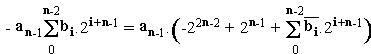
The product A.B is expressed as :
A.B = A.2n.bn + A.2n-1.bn-1
+
+ A.20.b0
The structure of Figure 6.37 is suited only for positive operands. If the operands are negative and coded in 2s-complement :
![[Zoom]](Figure-6.37.gif)
![[Zoom]](Figure-6.38.gif)
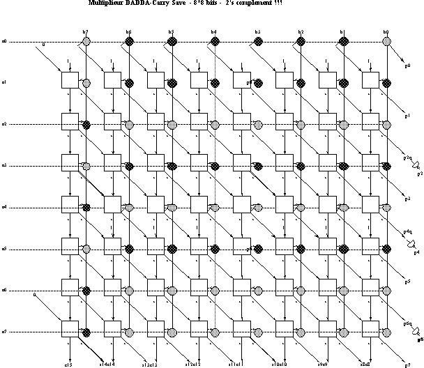
Figure 6.38 and Figure 6.40 use the symbols given in Figure 6.39 where CMUL1 and CMUL2 are two generic cells consisting of an adder without the final inverter and with one input connected to an AND or NAND gate. A non optimised (in term of transistors) multiplier would consist only of adder cells connected one to another with AND gates generating the partial products. In these examples, the inverters at the output of the adders have been eliminated and the parity of the bits has been compensated by the use of CMUL1 or CMUL2.
Let us consider 2 numbers A and B :
 (64), (65)
The product A.B is given by the following equation :
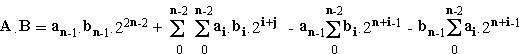 (66)
(66)We see that subtractor cells must be used. In order to use only adder cells, the negative terms may be rewritten as :
 (67)
(67)By this way, A.B becomes :
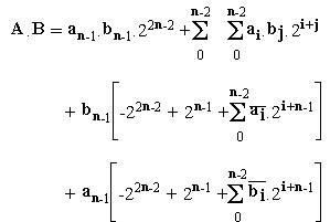 (68)
(68)The final equation is :
 (69)
(69)because :
A and B are n-bits operands, so their product is a 2n-bits number. Consequently, the most significant weight is 2n-1, and the first term -22n-1 is taken into account by adding a 1 in the most significant cell of the multiplier.
![[Zoom]](Figure-6.41.gif)
![[Zoom]](Figure-6.42.gif)
![[Zoom]](Figure-6.43.gif)
![[Zoom]](Figure-6.44.gif)
There are several ways to obtain the logarithm of a number : look-up
tables, recursive algorithms or the segmentation of the logarithmic curve
[Hoef91]. The segmentation method : The basic idea is to approximate the
logarithm curve with a set of linear segments.
If y = Log2 (x) (72)
an approximation of this value on the segment ]2n+1 , 2n[
can be made using the following equation :
y = ax + b = (![]() y
/
y
/ ![]() x
).x + b = [1 / (2n+1 - 2n)].x + n-1 = 2-n
x + (n-1) (73)
x
).x + b = [1 / (2n+1 - 2n)].x + n-1 = 2-n
x + (n-1) (73)
What is the hardware interpretation of this formula?
If we take xi = (xi7, xi6, xi5, xi4, xi3, xi2, xi1, xi0), an integer coded with 8 bits, its logarithm will be obtained as follows. The decimal part of the logarithm will be obtained by shifting xi n positions to the right, and the integer part will be the value where the MSB occurs.
For instance if xi is (0,0,1,0,1,1,1,0) = 46, the integer part of the logarithm is 5 because the MSB is xi5 and the decimal part is 01110. So the logarithm of xi equals 101.01110 = 5.4375 because 01110 is 14 out of a possible 32, and 14/32 = 0.4275
Table 9 illustrates this coding. Once the coding of two linear words has been performed, the addition of the two logarithms can be done. The last operation to be performed is the antilogarithm of the sum to obtain the value of the final product.
Using this method, a 11.6% error on the product of two binary operands (i.e. the sum of two logarithmic numbers) occurs. We would like to reduce this error without increasing the complexity of the operation nor the complexity of the operator. Since the transfomations used in this system are logarithms and antilogarithms, it is natural to think that the complexity of the correction systems will grow exponentially if the error approaches zero. We analyze the error to derive an easy and effective way to increase the accuracy of the result.
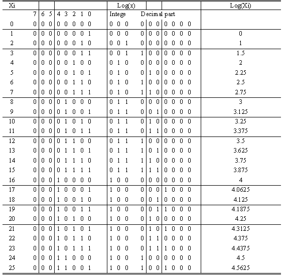
Figure 6.45 describes the architecture of the logarithmic multiplier with the different variables used in the system.
![[Zoom]](Figure-6.45.gif)
Error analysis: Let us define the different functions used in this system.
The logarithm and antilogarithm curves are approximated by linear segments. They start at values which are in powers-of-two and end at the next power-of- two value. Figure 6.46 shows how a logarithm is approximated. The same is true for the antilogarithm.
![[Zoom]](Figure-6.46.gif)
By adding the unique value 17*2-8 to the two logarithms an improvement of 40% is achieved on the maximum error. The maximum error comes down from 11.6% to 7.0%, an improvement of 40% compared with a system without any correction. The only cost is the replacement of the internal two input adder by a three input adder.
A more complex correction system which leads to better precision but at a much higher hardware cost is possible.
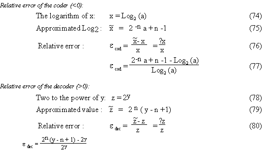
In Table 10 we suggest a system which would choose one correction among three depending on the value of the input bits. Table 10 can be read as the values of the logarithms obtained after the coder for either a1 or a2. The penultimate column represents the ideal correction which should be added to get 100% accuracy. The last column gives the correction chosen among three possibilities: 32, 16 or 0.
Three decoding functions have to be implemented for this proposal. If the exclusive -OR of a-2 and a-3 is true, then the added value is 32*2-8. If all the bits of the decimal part are zero, then the added value is zero. In all other cases the added value is 16*2-8.
This decreases the average error. But the drawback is that the maximum error will be minimized only if the steps between two ideal corrections are bigger than the unity step. To minimize the maximum error the correcting functions should increase in an exponential way. Further research could be performed in this area.
Definition
Let F be a set of elements on which two binary operations called addition "+" and multiplication".", are defined. The set F together with the two binary operations + and . is a field if the following conditions are satisfied:
a . ( b + c ) = a . b + a . c
A field with finite number of elements is called a finite field.
Let us consider the set {0,1} together with modulo-2 addition and multiplication. We can easily check that the set {0,1} is a field of two elements under modulo-2 addition and modulo-2 multiplication.field is called a binary field and is denoted by GF(2).
The binary field GF(2) plays an important role in coding theory [Rao74] and is widely used in digital computers and data transmission or storage systems.
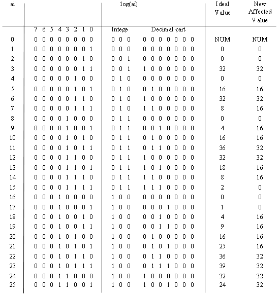
Another example using the residue to the base [Garn59] is given below. Table 11 represents the values of N, from 0 to 29 with their representation according to the residue of the base (5, 3, 2).The addition and multiplication of two term in this base can be performed according to the next example:
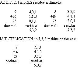
The most interesting property in these systems is that there is no carry propagation inside the set. This can be attractive when implementing into VLSI these operators
This
chapter
edited
by
D.
Mlynek