
![[previous]](../left.gif)
![[Table of Contents]](../toc.gif)
![[next]](../right.gif)
Digital signal processing is concerned with the representation of signals in digital form and the transformation or processing of such signal representation using numerical computation.
Sophisticated signal processing functions can be realized using digital techniques – numerous important signal processing techniques are difficult or impossible to implement using analog (continuous time) methods. Their reprogrammability is a strong advantage over conventional analog systems. Furthermore digital systems are inherently more reliable, more compact, and less sensitive to environmental conditions and component aging than analog systems. The digital approach allows the possibility of time-sharing (or multiplexing) a given DSP microprocessor among a number of different signal processing functions.
Since the invention of the transistor and integrated circuit, digital signal processing functions have been implemented on many hardware platforms ranging from special-purpose architectures to general-purpose computers. One of the earliest descriptions of a special-purpose hardware architecture for digital filtering was described by Bell Labs in 1968.[1] The problem with such architectures, however, is their lack of flexibility. In order to realize a complete application, one needs to be able to perform functions that go beyond simple filtering such as control, adaptive coefficient generation, and non-linear functions such as detection.
The solution is to use an architecture that is more like a general-purpose computer, but which can perform basic signal processing operations very efficiently. This means satisfying the following criteria:
In the 1960s and 1970s, multiple chips or special-purpose computers were designed for computing DSP algorithms efficiently. These systems were too costly to be used for anything but research or military radar applications. It was not until all of this functionality (arithmetic, addressing, control, I/O, data storage, control storage) could be realized on a single chip that DSP could become an alternative to analog signal processing for the wide span of applications that we see today.
In the late 1970s large-scale integration technology reached the point of maturity that it became practical to consider realizing a single chip DSP. Several companies developed products along these lines including AMI, Intel, NEC, and Bell Labs.
The first DSP generation
AMI S2811
AMI announced a "Signal Processing Peripheral" in 1978.[1] The S2811 was designed to operate in conjunction with a microprocessor such as the 6800 and depended upon it for initialization and configuration.[2] With a small, nonexpandable program memory of only 256 words, the S2811 was intended to be used to offload some math intensive subroutines from the microprocessor. Therefore, as a peripheral, it could not "stand alone" as could DSPs from Bell Labs, NEC, and other companies. The part was to be implemented in an exotic process technology called "V-groove." Availability of first silicon was after 1979 and was never used in any volume product.[3]
Intel 2920
Intel announced an "Analog Signal Processor," the 2920, at the 1979 Institute of Electrical and Electronics Engineers (IEEE) Solid State Circuits Conference.[4] A unique feature of this device was the on-chip analog/digital and digital/analog converter capability. The drawback was the lack of a multiplier. Multiplication was performed by a series of instructions involving shifting (scaling) and adding partial products to an accumulator. Multiplication of two variables was even more involved—requiring conditional instruction execution.
In addition, the mechanism for addressing memory was limited to direct addressing. The program could not perform branching.[5] As such, while it could perform some signal processing calculations a little more efficiently than a general-purpose microprocessor, it greatly sacrificed flexibility and has little resemblance to today's single-chip DSP. Too slow for any complete application, it was used as a component for part of a modem.[6]
NECµPD7720
NEC announced a digital signal processor, the 7720, at the IEEE Solid State Circuits Conference in February 1980 (the same conference that Bell Labs disclosed its first single-chip DSP). The 7720 does have all of the attributes of a modern single chip DSP as described above. However, devices and tools were not available in the U.S. until as late as April 1981.[7]
The Bell Labs DSP1
The genesis of Bell Labs' first single-chip DSP was the recommendation of a study group that began to consider the possibility of developing a multipurpose, large-scale integration circuit for digital signal processing in January 1977.[8] Their report, issued in October 1977, outlined the basic elements of a minimal DSP architecture which consisted of multiplier/accumulator, addressing unit, and control. The plan was for the I/O, data, and control memories to be external to the 40-pin DIP until large-scale integration technology could support their integration. The spec was completed in April 1978 and the design a year later. First samples were tested in May 1979. By October, devices and tools were distributed to other Bell Labs development groups. It became a key component in AT&T's first digital switch, 5ESS, and many other telecommunications products. Devices with this architecture are still in manufacture today.
The first Bell Labs DSP was different from what was in the report. The DSP1 contained all of the functional elements found in today's DSPs including a multiplier-accumulator (MAC), parallel addressing unit, control, control memory, data memory, and I/O. It fully meets the above criteria for a single-chip DSPs.
The DSP1 was first disclosed outside AT&T at the IEEE Solid State Circuits Conference in February 1980.[9] A special issue of the BellSystem Technical Journal was published in 1981 which described the architecture, tools, and nine fully developed telecommunications applications for the device.[10]
The following table summarizes the evolution of DSPs:
|
Date |
Features |
Example processors |
|
First generation : 1979 - 1985 |
Harvard architecture, hardwired multiplier |
NECµPD7720, Intel 2920, Bell Labs DSP1, Texas Instruments TMS320C10 |
|
Second generation: 1985 - 1988 |
Concurrency, multiple busses, on-chip memory |
TMS320C25, MC56001, DSP16 (AT&T) |
|
Third generation: 1988 - 1992 |
On-chip floating point operations |
TMS320C30, MC96002, DSP32C (AT&T), |
|
Fourth generation: 1992 - 1997 |
Multi-processing features Image and video processors Low-power DSPs (AT&T) |
TMS320C40&50 TMS320C80 |
|
Fifth generation: 1997 – |
VLIW |
TMS320C6x, Philips TriMedia, Motorola Starcore |
Digital signal processing in general, and DSP processors in particular, are used in a wide variety of applications from military radar systems to consumer electronics. Naturally, no one processor can meet the needs of all applications. Criteria such as performance, cost, integration, ease of development, power consumptions are key points to examine when designing or selecting a particular DSP for a class of applications. The table below summarizes different processor applications.
Table 1. Common DSP algorithms and typical applications ([11])
|
DSP Algorithm |
System Application |
|
Speech coding and decoding |
Digital cellular phones, personal communications systems, multimedia computers, secure communication |
|
Speech encryption and decryption |
Digital cellular phones, personal communications systems, secure communication |
|
Speech recognition |
Advanced user interfaces, multimedia workstation, robotics, automotive applications, digital cellular phones,…. |
|
Speech synthesis |
Multimedia PCs, advanced user interface, robotics |
|
Speaker identification |
Security, multimedia workstations, advanced user interfaces |
|
Hi-fi audio encoding and decoding |
Consumer audio & video, digital audio broadcast, professional audio, multimedia computers |
|
Modem algorithms |
Digital cellular phones, personal communication systems, digital audio broadcast, digital signalling on cable TV, multimedia computers, wireless computing, navigation, data/fax modems, secure communications |
|
Noise cancellation |
Professional audio, advanced vehicular audio, industrial applications |
|
Audio equalization |
Consumer audio, professional audio, advanced vehicular audio, music |
|
Ambient acoustics emulation |
Consumer audio, professional audio, advanced vehicular audio, music |
|
Audio mixing and editing |
Professional audio, music, multimedia computers |
|
Sound synthesis |
Professional audio, music, multimedia computers, advanced user interfaces |
|
Vision |
Security, multimedia computers, advanced user interfaces, instrumentation, robotics, navigation |
|
Image compression and decompression |
Digital photography, digital video, multimedia computers, video-over-voice, consumer video |
|
Image composition |
Multimedia computers, consumer video, advanced user interfaces, navigation |
|
Beamforming |
Navigation, medical imaging, radar/sonar, signals intelligence |
|
Echo cancellation |
Speakerphones, modems, telephone switches |
|
Spectral Estimation |
Signals intelligence, radar/sonar, professional audio, music |
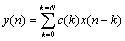
The Finite Impulse Response filter (FIR) is a convenient way to introduce features needed in typical DSP systems. The FIR filter is described by the following equation:
The following diagram shows an FIR filter. This illustrates the basic DSP operations:
Each of these operations has its own special set of requirements:
additions and multiplications require to:
delays require to:
array handling requires to:
To suit these fundamental operations DSP processors often have:
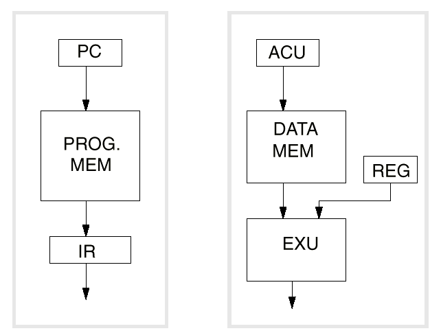
The simplest processor memory structure is a single bank of memory, which the processor accesses through a single set of address and data lines. This structure which is common among non-DSP processors is referred as the Von Neuman architecture. In this implementation, data and instruction are stored in the same single bank and one access to memory is performed during each instruction cycle. As seen previously to perform a typical operation for a DSP is to have a MAC operation executed in one cycle. This operation requires to fetch two data from memory, multiply them together and add the result to the previous result. With such a Von Neuman model it is not possible to fetch the instruction and the data in the same cycle. This is one reason why conventional processors do not perform well on DSP applications in general.
The solution to solve memory accesses is known as the Harvard architecture and the modified Harvard architecture. The following diagram shows the Harvard architecture. The program counter fetch an instruction from the program memory using the program counter and stores it in the instruction register. In parallel, the Address Calculation Unit fetch one operand from the memory and feed the execution unit with it. This simple architecture allows one instruction word and one data word to be fetched in a single cycle. This system requires 4 buses: 2 address bus and 2 data bus.
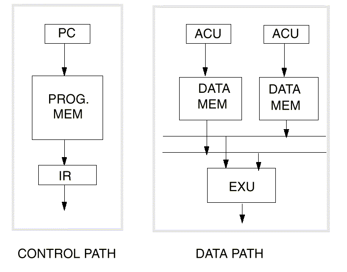
The next picture represents the modified Harvard architecture. Two data are now fetched in the memory in a single cycle. Since it is not possible to access the same memory in the same cycle, this implementation requires three memory banks: a program memory bank and two data memory bank commonly designed X and Y, each with its own set of buses: address and data.
The data path of a DSP processor is where the vital arithmetic manipulations of signals take place. DSP processor data paths are highly specialized to achieve high performance on the types of computation most common in DSP applications, such as multiply-accumulate operations. Registers, Adders, Multipliers, Comparators, Logic operators, Multiplexers, Buffers represent 95% of a typical DSP data path.
Multiplier
A single-cycle multiplier is the essence of a DSP since multiplication is an essential operation in all DSP applications. An important distinction between multipliers in DSPs is the size of the product according to the size of the operands. In general, multiplying two n-bit fixed-point numbers requires a 2xn bits to represent the correct result. For this reason DSPs have in general a multiplier, which is twice the word length of the native operands.
Accumulators Registers
Accumulators registers hold intermediate and final results of multiply-accumulate and other arithmetic operations. Most DSP processors have two or more accumulators. In general, the size of the accumulator is larger than the size of the result of a product. These additional bits are called guard bits. These bits allow accumulating values without the risk of overflow and without rescaling. N additional bits allow up to 2n accumulations to be performed without overflow. Guards bits method is more advantageous than scaling the multiplier product since it allows the maximum precision to be retained in intermediate steps of computations.
ALU
Arithmetic logic units implement basic arithmetic and logical operations. Operations such as addition, subtraction, and, or are performed in the ALU.
Shifter
In fixed-point arithmetic, multiplications and accumulations often induce a growth in the bit width of results. Scaling is then necessary to pass results from stage to stage and is performed through the use of shifters.
The following diagram shows the Motorola 56002 Data Path
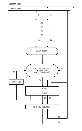
Data ALU input Registers
X1, X0, Y1, and Y0 are four 24-bit, general-purpose data registers. They can be treated as four independent, 24-bit registers or as two 48-bit registers called X and Y, developed by concatenating X1:X0 and Y1:Y0, respectively. X1 is the most significant word in X and Y1 is the most significant word in Y. The registers serve as input buffer registers between the X Data Bus or Y Data Bus and the MAC unit. They act as Data ALU source operands and allow new operands to be loaded for the next instruction while the current instruction uses the register contents. The registers may also be read back out to the appropriate data bus to implement memory-delay operations and save/restore operations for interrupt service routines.
MAC and Logic Unit
The MAC and logic unit shown in the figure below conduct the main arithmetic processing and perform all calculations on data operands in the DSP.
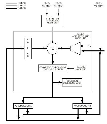
For arithmetic instructions, the unit accepts up to three input operands and outputs one 56-bit result in the following form: extension:most significant product:least significant product (EXT:MSP:LSP). The operation of the MAC unit occurs independently and in parallel with XDB and YDB activity, and its registers facilitate buffering for Data ALU inputs and outputs. Latches on the MAC unit input permit writing an input register which is the source for a Data ALU operation in the same instruction. The arithmetic unit contains a multiplier and two accumulators. The input to the multiplier can only come from the X or Y registers (X1, X0, Y1, Y0). The multiplier executes 24-bit x 24-bit, parallel, twos-complement fractional multiplies. The 48-bit product is right justified and added to the 56-bit contents of either the A or B accumulator. The 56-bit sum is stored back in the same accumulator. An 8-bit adder, which acts as an extension accumulator for the MAC array, accommodates overflow of up to 256 and allows the two 56-bit accumulators to be added to and subtracted from each other. The extension adder output is the EXT portion of the MAC unit output. This multiply/accumulate operation is not pipelined, but is a single-cycle operation. If the instruction specifies a multiply without accumulation (MPY), the MAC clears the accumulator and then adds the contents to the product.
In summary, the results of all arithmetic instructions are valid (sign-extended and zero-filled) 56-bit operands in the form of EXT:MSP:LSP (A2:A1:A0 or B2:B1:B0). When a 56-bit result is to be stored as a 24-bit operand, the LSP can be simply truncated, or it can be rounded (using convergent rounding) into the MSP. Convergent rounding (round-to-nearest) is performed when the instruction (for example, the signed multiply-accumulate and round (MACR) instruction) specifies adding the multiplier’s product to the contents of the accumulator. The scaling mode bits in the status register specify which bit in the accumulator shall be rounded. The logic unit performs the logical operations AND, OR, EOR, and NOT on Data ALU registers. It is 24 bits wide and operates on data in the MSP portion of the accumulator. The LSP and EXT portions of the accumulator are not affected. The Data ALU features two general-purpose, 56-bit accumulators, A and B. Each consists of three concatenated registers (A2:A1:A0 and B2:B1:B0, respectively). The 8-bit sign extension (EXT) is stored in A2 or B2 and is used when more than 48-bit accuracy is needed; the 24-bit most significant product (MSP) is stored in A1 or B1; the 24-bit least significant product (LSP) is stored in A0 or B0. Overflow occurs when a source operand requires more bits for accurate representation than are available in the destination. The 8-bit extension registers offer protection against overflow. In the DSP56K chip family, the extreme values that a word operand can assume are - 1 and + 0.9999998. If the sum of two numbers is less than - 1 or greater than + 0.9999998, the result (which cannot be represented in a 24 bit word operand) has underflowed or overflowed. The 8-bit extension registers can accurately represent the result of 255 overflows or 255 underflows. Whenever the accumulator extension registers are in use, the V bit in the status register is set.
Automatic sign extension occurs when the 56-bit accumulator is written with a smaller operand of 48 or 24 bits. A 24-bit operand is written to the MSP (A1 or B1) portion of the accumulator, the LSP (A0 or B0) portion is zero filled, and the EXT (A2 or B2) portion is sign extended from MSP. A 48-bit operand is written into the MSP:LSP portion (A1:A0 or B1:B0) of the accumulator, and the EXT portion is sign extended from MSP. No sign extension occurs if an individual 24-bit register is written (A1, A0, B1, or B0).When either A or B is read, it may be optionally scaled one bit left or one bit right for block floating-point arithmetic. Sign extension can also occur when writing A or B from the XDB and/or YDB or with the results of certain Data ALU operations (such as the transfer conditionally (Tcc) or transfer Data ALU register (TFR) instructions).
Overflow protection occurs when the contents of A or B are transferred over the XDB and YDB by substituting a limiting constant for the data. Limiting does not affect the content of A or B – only the value transferred over the XDB or YDB is limited. This overflow protection occurs after the content of the accumulator has been shifted according to the scaling mode. Shifting and limiting occur only when the entire 56-bit A or B accumulator is specified as the source for a parallel data move over the XDB or YDB. When individual registers A0, A1, A2, B0, B1, or B2 are specified as the source for a parallel data move, shifting and limiting are not performed.
The accumulator shifter is an asynchronous parallel shifter with a 56-bit input and a 56-bit output that is implemented immediately before the MAC accumulator input. The source accumulator shifting operations are as follows:
The ability to generate new addresses efficiently is a characteristic feature of DSP processors. Most DSP processors include one or more special address generation units (AGUs) that are dedicated to calculating addresses. An AGU can perform one or more special address generation per instruction cycle without using the processor main data path. The calculation of addresses takes place in parallel with arithmetic operations on data, improving processor performance.
On of the main addressing mode is the register-indirect addressing. The data addressed is in memory and the address of the memory location containing the data is held in a register. This gives a natural way to work with arrays of data. Another advantage is the efficiency from an instruction-set point of view since it allows powerful and flexible addressing with relatively few bits in the instruction word.
Whenever an operand is fetched from memory using register indirect addressing, the address register can be incremented to point to the next needed value in the array. The following table summarizes most common increment method in DSPs:
|
*rP |
register indirect |
read the data pointed to by the address in register rP |
|
*rP++ |
postincrement |
Having read the data, postincrement the address pointer to point to the next value in the array |
|
*rP-- |
postdecrement |
Having read the data, postdecrement the address pointer to point to the previous value in the array |
|
*rP++rI |
register postincrement |
Having read the data, postincrement the address pointer by the amount held in register rI to point to rI values further down the array |
|
*rP++rIr |
bit reversed (FFT) |
having read the data, postincrement the address pointer to point to the next value in the array, as if the address bits were in bit reversed order |
An additional convenient feature in AGU is the presence of modulo addressing modes. It is extensively used for circular addressing. Instead of comparing the address to a calculated value to see whether or not the end of the buffer has been reached, dedicated registers are used to automatically perform this check and take necessary actions (i.e. reset the register to the start address of the buffer).
The following picture represents the address generation unit of the Motorola 56002
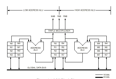
This AGU uses integer arithmetic to perform the effective address calculations necessary to address data operands in memory, and contains the registers used to generate the addresses. It implements linear, modulo, and reverse-carry arithmetic, and operates in parallel with other chip resources to minimize address-generation overhead. The AGU is divided into two identical halves, each of which has an address arithmetic logic unit (ALU) and four sets of three registers. They are the address registers (R0 - R3 and R4 - R7), offset registers (N0 - N3 and N4 - N7), and the modifier registers (M0 - M3 and M4 - M7). The eight Rn, Nn, and Mn registers are treated as register triplets — e.g., only N2 and M2 can be used to update R2. The eight triplets are R0:N0:M0, R1:N1:M1, R2:N2:M2, R3:N3:M3, R4:N4:M4, R5:N5:M5, R6:N6:M6, and R7:N7:M7.
The two arithmetic units can generate two 16-bit addresses every instruction cycle — one for any two of the XAB, YAB, or PAB. The AGU can directly address 65,536 locations on the XAB, 65,536 locations on the YAB, and 65,536 locations on the PAB. The two independent addresses ALUs work with the two data memories to feed the data ALU two operands in a single cycle. Each operand may be addressed by a Rn, Nn, and Mn triplet.
Most DSP processors provides on-chip peripherals and interfaces to allow the DSP to be used in an embedded system with a minimum amount of external hardware to support its operation and interfacing.
Serial port
A serial interface transmits and receives data one bit at a time. These ports have a variety of applications like sending and receiving data samples to and from A/D and D/A converters and codecs, sending and receiving data to and from other microprocessors or DSPs, communicating with other hardware. The two main categories are synchronous and asynchronous interface. The synchronous serial ports transmit a bit clock signal in addition to the serial bits. The receiver uses this clock to decide when to sample received data. On the opposite, asynchronous serial interfaces do not transmit a separate clock signal; they rely on the receiver deducing a clock signal from the data itself.
Direct extension of serial interfaces leads to parallel ports where data are transmitted in parallel instead of sequentially. Faster communication is obtained through costly additional pins.
Host Port
Some DSPs provide a host port for connection to a general-purpose processor or another DSP. Host ports are usually specialized 8 or 16 bit bi-directional parallel ports that can be used to transfer data between the DSP and the host processor.
Link ports or communications ports
This kind of port is dedicated to multiprocessor operations. It is in general a parallel port intended for communication between the same types of DSPs.
Interrupt controller
An interrupt is an external event that causes the processor to stop executing its current program and branch to a special block of code called an interrupt service routine. Typically this code deals with the origin of the interrupt and then returns from the interrupt. There are different interrupt sources:
On-chip peripherals: serial ports, timers, DMA,…
External interrupt lines: dedicated pins on the chip to be asserted by external circuitry
Software interrupts: also called exceptions or traps, these interrupts are generated under software control or occurs for example for floating-point exceptions (division-by-zero, overflow and so on).
DSPs associates interrupts with different memory locations. These locations are called interrupt vectors. These vectors contain the address of the interrupt routines. When an interrupt occurs, the following scenario is often encountered:
Priority levels can be assigned to the different interrupt through the use of dedicated registers. An interrupt is acknowledged when its priority level is strictly higher that current priority level.
Timers
Programmable timers are often used as a source of periodic interrupts. Completely software-controlled to activate specific tasks at chosen times. It is generally a counter that is preloaded with a desired value and decremented on clock cycles. When zero is reached, an interrupt is issued.
DMA
Direct Memory Access is a technique whereby data can be transferred to or from the processor’s memory without the involvement of the processor itself. DMA is commonly used to provide improved performance with input/output devices. Rather than have the processor read data from an I/O device and copy the data into memory or vice versa, a separate DMA controller can handle such transfers in parallel. Typically, the processor loads the DMA controller with control information including the starting address for the transfer, the number of words to be transferred, the source and the destination. The DMA controller uses the bus request pin to notify the DSP core that it is ready to make a transfer to or from external memory. The DSP core completes its current instruction, releases control of external memory and signals the DMA controller via the bus grant pin that the DMA transfer can proceed. The DMA controller then transfers the specified number of data words and optionally signals completion through an interrupt. Some processor can also have multiple channels DMA managing DMA transfers in parallel.
• FIR/IIR filters
• FFTs
• convolution
• dot product
The term "superscalar" is commonly used to designate architectures that enable more than one instruction to be executed per clock cycle
Nowadays multimedia architectures, supported by the continuous improvement in technologies, are rapidly moving towards highly parallel solutions like SIMD and VLIW machines. What do these acronyms mean ?
SIMD stands for Single Instruction on Multiple Data. In simple words it is possible to say that the architecture has a single program control unit that fetches and decodes the program instructions to multiple execution units, i.e. multiple sets of datapaths, registers and data memories. Of course a SIMD architecture can be realized by a multiprocessor configuration, but the exploitation of deep submicron technologies has made possible to integrate such architectures in a single chip. It is easy at this point to imagine each execution unit to be driven by different program control units, permitting the possibility to execute in parallel different instructions of the same program or different programs at the same time; in this case the resulting architecture is called Multiple Instructions on Multiple Data (MIMD). Again a MIMD machine can be implemented by a multiprocessor structure or integrated in a single chip.
Historically the first examples of the so-called multiple-issue machines were typified in the early '80s, and they were called VLIW machines (for Very Long Instruction Word). These machines exploit an instruction word consisting of several (up to 8) instruction fragments. Each fragment controls a precise execution unit; in this way the register set must be multiported to support simultaneous access, because the multiple instructions could need to share the same variables. In order to accommodate the multiple instruction fragments, the instruction word is often over 100 bits long. [12]
The reasons that push towards these parallel approaches are essentially two; first of all many scientific and processing algorithms either for calculus or, more recently, for communication and multimedia applications contain a high degree of parallelism. Secondly a parallel architecture is a cost-effective way to compute (when the program is parallelizable), since internal and on-chip communications are much faster and much more efficient than external communication channels.
On the other hand parallel architectures bring with them a number of problems and new challenges that are not present in simple processors. First of all, if it is true that many programs are parallelizable, extensive researches have shown that often the level of parallelism that can be achieved is theoretically not greater than 3; this means that on actual architectures the speedup factor is not greater than 2. Based upon this, it would seem that in the absence of significant compiler breakthroughs available speedup is limited. A second problem concerns memories and registers; highly parallel routines require a high memory access rate, and then a very difficult optimization for register set, cache memory and data buses in order to feed the necessary amount of data into the execution units. Finally, such complex architectures with hardly optimized datapaths and data transfers are very difficult to program. Normally DSP programmers used to develop applications directly in assembly language, very similar for some aspects to the natural sequential way of thinking of the human beings and specifically conceived for smart optimizations. Machines like the MIMD and VLIW ones are not programmable in assembly anymore, and then processor designers have to spend a great amount of resources (often more than the time to develop the chip itself) in order to provide the Software Development Kits able to exploit the full potential of the processor, taking care of every aspect from the powerful optimization techniques until understandable user interfaces.
More recent attempts at multiple-issue processors have been directed at rather lower amounts of concurrency than in the first VLIW architectures (4-5 parallel execution blocks). Three examples of this new generation of superscalar machines will be briefly discussed in the next subsections, underlying architectural aspects and specific solutions to deal with the problems of parallelization.
The Pentium processor with multimedia extensions
The Pentium processor explicitly supports multimedia, since the introduction of the so-called MMX (MultiMedia eXtension) family. The well-known key enhancement of this new technology consists of exploiting the 64-bit floating point registers of the processor to "pack" 8-, 16-, or 32-bit data, that can be processed in parallel by a SIMD operating unit. Fifty-seven new instructions are implemented in the processor in order to exploit these new functionalities, and among them "multiply and add", the basic operation in the case of digital convolutions (FIR filters) or FFT algorithms. [13] Two considerations can be made about this processor. First of all the packed data are fixed point, and then the use of these extensions for a DSP oriented task limits the use of the floating point arithmetic; conversely a full use of floating-point operations does not allow any boost in performance in comparison with the common Pentium family.
Moreover MMX technology has been conceived to specifically support multimedia algorithms, but at the same time to completely preserve code compatibility with previous processors; in this way an increased potential in fixed-point processing power is not supported by the necessary memory and bus re-design, and then it is often not possible to "feed" the registers with the correct data. Extensive tests conducted after the disclosing of the MMX technology have shown that for typical video application it is often a hard matter to achieve a speedup factor of the 50%.
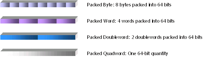
Figure 1. How the Pentium MMX exploits the 64-bit floating-point registers to "pack" data in parallel and send them to a SIMD execution unit
The TriMedia processor
Another multimedia processor other than Intel MMX that is growing in interest is the TriMedia by Philips Electronics. This chip is not designed as a completely general purpose CPU, but with the double functionality of CPU and DSP in the same chip, and its core processing master unit presents a VLIW architecture.
The key features of TriMedia are:
The architecture of the TriMedia is shown in figure 2.
The real DSP processing must be implemented in the master CPU/DSP, which is also responsible for the whole algorithm direction. This unit is a 32-bit floating-point, 133 MHz general-purpose unit whose VLIW instructions can address up to five instructions out of the 27 functional operations (integer and floating point, 2 multipliers and 5 ALUs).
The DSPCPU is provided with a 32 Kbytes Instruction cache memory and a dual port 16 Kbytes Data cache memory. [14]
TriMedia also provides a set of multimedia instructions, mostly targeted at MPEG-2 video decoding;
Figure 2 The TriMedia processor architecture
Some of the programming challenges for parallel architectures are solved in the DSPCPU through the concept of guarded conditional operations. An instruction takes the following form
R g : R dest = imul R src1 , R src2
In this instruction the integer multiplication of the two registers is put into the destination register under the condition contained in the "guard" register Rg. This allow to better control the optimization strategies of the parallel compiler, since for instance the problem of branches is relaxed and the result is accepted or not only at the last execution stage of the pipeline.
As mentioned above, complex processors/DSPs like TriMedia need a big amount of development tools and software support. For this reasons the TriMedia comes with a huge amount of tools to deal with the real-time kernel, the DSPCPU programming and the complete system exploitation.
The TriMedia Software Development Environment provides a comprehensive suite of system software tools to compile and debug multimedia applications, analyse and optimize performance, and simulate execution on the TriMedia processor. The main features are:
PUMA - Parallel Universal Music Architecture
A very interesting solution recently developed for advanced audio applications is the PUMA (Parallel Universal Music Architecture) DSP by Studer Professional Audio. This chip was conceived and realised in collaboration with the Integrated Systems Center (C3I) of the EPFL.
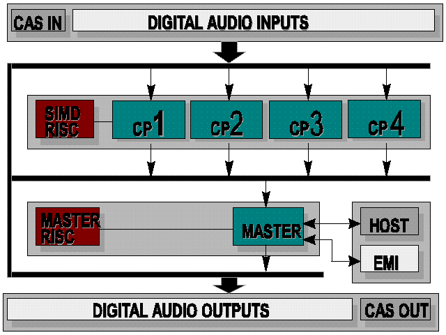
This integrated circuit is designed and optimized for digital mixing consoles; it is provided with 4 independent channel processors, and then with four 33-MHz, 24-bit fixed point multipliers and adders fully dedicated to data processing (another multiplier is provided in the master DSP, which is charged of the final data processing and directs the whole chip functionalities and I/O unities); the important feature of this chip relies in the multiple processing units that can work in parallel on similar blocks of data; each channel processor has its own internal data memory (256 24-bit words for each processor), the Master DSP and the Array DSP has independent program memories and program control units. The design of the I/O units deserved a great care: digital audio input and output are supported by 20 serial lines each; interprocessor communication is supported through fully independent units (the Cascade Data Input and Cascade Data Output) providing 64 channels on 8 lines at full processor speed. A general purpose DRAM/SRAM External Memory Interface and the External Host Interface permit memory extension and flexible programmability via an external host processor. The following figure shows the top-level architecture of the PUMA DSP.
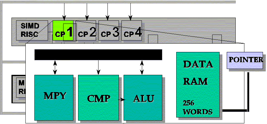
The following figure shows the internal datapath of each channel processor; three units can work in parallel in a single clock cycle: a 24x24-bit multiplier, a comparator and the general purpose ALU (adder, shifter, logical operations).
Puma design flow
To conclude it is interesting to spend a few words about the PUMA design flow, to understand how a modern and complex architecture, characterised by several million of transistors, can be practically realised.
First of all the functional specification of the processor is developed, defining functionalities, basic blocks and instruction set; at the same time the C-model of the architecture is implemented, in order to test with a simple methodology the algorithms and the architecture.
The second step is the VHDL description and simulation of the C-model at the RTL level, followed by the synthesis to the gate level. All of this was accomplished exploiting the Synopsys Design Compiler and Design Analyzer.
After that an optimization technique called hierarchical compiling is used: after setting the boundary constraints for the main blocks, the constraints for the inner blocks are derived hierarchically by the compiler, and this permits to relax the time paths everywhere it is not strictly necessary.
The preliminary place & route follows; then the parasitic parameters (R and C) for each wire are extracted, and the so called back-annotation, or in-place compilation is performed, in order to better adapt each load to the real netlist placement. The place & route was made by the Compass tool, the back-annotation again in Synopsys Design Compiler.
Finally the last place&route is made, and extensive simulations are performed for every part of the chip, in order to verify the timing of every specific operation. Now the design is ready for the foundry.
References
1. Nicholson, Blasco and Reddy, "The S2811 Signal Processing Peripheral," WESCOM Tech Papers, Vol. 22, 1978, pp. 1-12.
2. S2811 Signal Processing Peripheral, Advanced Product Description, AMI, May 1979.
3. Strauss, DSP Strategies 2000, Forward Concepts, Tempe, AZ, November 1996, p. 24.
4. Hoff and Townsend, "An analog input/output microprocessor for signal processing," ISSCC Digest of Tech. Papers, February 1979, p. 220.
5. 2920 Analog Signal Processor Design Handbook, Intel, Santa Clara, CA, August 1980.
6. Strauss, DSP Strategies 2000, Forward Concepts, Tempe, AZ, November 1996, p.24.
7. Brodersen, "VLSI for Signal Processing," Trends and Perspectives in Signal Processing, Vol. 1, No. 1, January 1981, p. 7.
8. Stanzione et al, "Final Report Study Group on Digital Integrated Signal Processors," Bell Labs Internal Memorandum, October 1977.
9. Boddie, Daryanani, Eldumtan, Gadenz, Thompson, Walters, Pedersen, "A Digital Signal Processor for Telecommunications Applications," ISSCC Digest of Technical Papers, February 1980, p.44.
10. Bell System Technical Journal, Vol. 60, No. 7, September 1981.
11. Phil Lapsley, Jeff Bier, Amit Shoham "DSP Processor Fundamentals, Arhitectures and Features", IEEE Press.
12. Michael J. Flynn "Computer Architecture. Pipelined and parallel processor design", Jones and Bartlett, 1995.
13. Peleg A., Wilkie S., Weiser U. Intel MMX for Multimedia PCs. Communications of the ACM, Vol. 40, No. 1, Jan 1997.
14. TM1000 Preliminary Data Book, Philips Electronics NAC, 1997.