Copyright Michael Karbo and ELI Aps., Denmark, Europe.
Chapter 25. From ISA to PCI Express
From about 1984 on, every PC had a standard bus which was used for I/O tasks. That was the ISA (Industry Standard Architecture) bus.
Right up until about 1999 there were still ISA slots in most PCs. In the later years, however, they were only kept for compatibility, so that plug-in cards of the old ISA type could be re-used. This was particularly the case for sound cards from SoundBlaster; they worked quite well on the ISA bus, and many games were programmed to directly exploit this type of hardware. It therefore took many years to get away from the ISA bus, but we have managed to now.
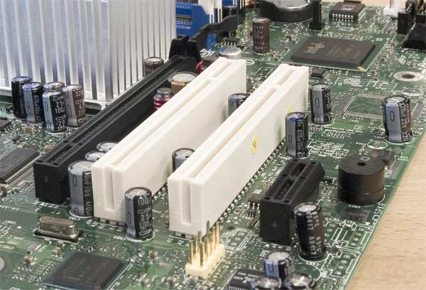
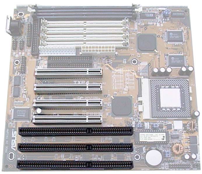 Fig. 165. Motherboard from 1998 with three
(black) ISA slots and four (white) PCI slots.
Fig. 165. Motherboard from 1998 with three
(black) ISA slots and four (white) PCI slots.
History of the ISA bus
The ISA bus is thus the I/O bus which survived the longest. Here is some information about it:
|
ISA was an improvement to IBMs original XT bus (which was only 8 bits wide) IBM used the protected name AT Bus, but in everyday conversation it was called the ISA bus. |
|
The ISA bus was 16 bits wide, and ran at a maximum clock frequency of 8 MHz. |
|
The bus has a theoretical bandwidth of about 8 MB per second. However in practise it never exceeds about 1-2 MB/sec. partly because it takes 2-3 of the processors clock pulses to move a packet (16 bits) of data. |
Fig. 166. The ISA bus is not used much today, but it had enormous significance in the years up until the middle of the 1990s.
The ISA bus had two faces in the old PC architecture:
Sluggish performance
One of the reasons the ISA bus was slow was that it only had 16 data channels. The 486 processor, once it was introduced, worked with 32 bits each clock pulse. When it sent data to the ISA bus, these 32-bit packets (dwords or doublewords) had to be split into two 16-bit packets (two words), which were sent one at a time, and this slowed down the flow of data.
|
Bus |
Time per |
Amount of data per |
|
ISA |
375 ns |
16 bits |
|
PCI |
30 ns |
32 bits |
Fig. 167. The PCI bus was a huge step forward.
The ISA bus was not intelligent either, since it was in principle the CPU which controlled all the work the bus was doing. This meant the CPU could only begin a new task when the transfer was complete. You may perhaps have experienced yourself, that when your PC works with the floppy disk drive the rest of the PC virtually grinds to a halt. Thats the ISA buss fault, and it therefore only happens on older PCs.
These small delays are called wait states. If an ISA adapter cannot keep up with the data it is receiving, it sends wait states to the CPU. These are signals to the CPU telling it to do nothing. A wait state is a wasted clock pulse the CPU skips over a clock pulse, without doing anything. Thus a slow ISA adapter could choke any PC.
Another problem was that the ISA bus often played up when you were installing an expansion card (e.g. a sound card). Many of the problems were associated with the handling of IRQs and DMA channels (I will explain these terms later), which often had to be done by hand with the old ISA bus.
Every device takes up one particular IRQ, and possibly a DMA channel, and conflicts often arose with other devices. It was a big relief when Intel, in the late 1990s, finally dropped the ISA bus and replaced it with the smart USB bus.
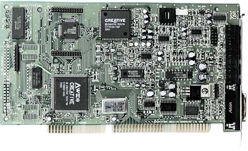 Fig. 168. ISA based Sound Blaster sound card.
The MCA, EISA and VL buses
The ISA bus was too slow, and the solution was to develop new standards for I/O devices. In 1987-88, two new I/O buses were put forward. First, IBM brought out their technologically advanced MCA bus. But since it was patented, a number of other companies pooled together to create the equivalent EISA bus.
But neither MCA or EISA had a big impact on the clone market. We were stuck with the ISA bus up until 1993, when the VL bus finally became reasonably widespread. It was a genuine local bus, which means it worked synchronously with the system bus. The VL bus was very primitive; it was really just an extension of the system bus.
The VL bus never managed to have a big impact, because almost at the same time, the robust and efficient PCI bus broke through. The various I/O buses are summarised below:
|
Bus |
Description |
|
PC-XT |
Synchronous 8-bit bus which followed the CPU clock
frequency of 4.77 or 6 MHz. |
|
ISA (PC-AT) |
Simple, cheap I/O bus. |
|
MCA |
Advanced I/O bus from IBM (patented). Asynchronous, 32-bit, at 10 MHz. |
|
EISA |
Advanced I/O bus (non-IBM), used especially in network
servers. |
|
VESA Local Bus |
Simple, high-speed I/O bus. |
|
PCI |
Advanced, general, high-speed I/O bus. 32-bit, asynchronous, at 33 MHz. |
|
USB and Firewire, from 1998 |
Serial buses for external equipment. |
|
PCI Express |
A serial bus for I/O cards with very high speed.
Replaces PCI and AGP. |
Fig. 169. The PCs I/O buses, throughout the years.
The PCI bus
PCI stands for Peripheral Component Interconnect. The bus is an Intel product which is used in all PCs today, and also in other computers, as the PCI bus is processor independent. It can be used with all 32-bit and 64-bit processors, and is therefore found in many different computer architectures.
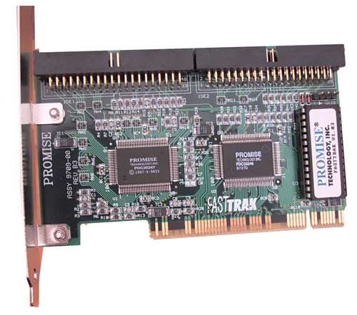 Fig. 170. PCI bus adapter.
At the same time, the bus is compatible with the ISA bus to a certain extent, since PCI devices can react to ISA bus signals, create the same IRQs etc. One consequence of this was that Sound Blaster compatible sound cards could be developed, which was very important in the middle of the 1990s. In optimal conditions, the PCI bus sends one packet of data (32 bits) each clock pulse. The PCI bus therefore has a maximum bandwidth of 132 MB per second, as shown below:
|
Clock |
33 MHz |
|
Bus width: |
32 bits |
|
Bandwidth: |
32 bits
x 33,333,333 clock pulses/second = |
Fig. 171. The maximum bandwidth of the PCI bus.
There is also a more powerful versions of the PCI standard, which provides greater bandwidth, but most motherboards still use the original version. The PCI bus has a buffer which operates between the CPU and the peripheral devices (a kind of cache RAM). This allows the CPU to deliver its data to the buffer, and then perform other tasks. The bus looks after the rest of the delivery itself at its own pace. Alternatively, PCI adapters can also deliver data to the buffer, whether or not the CPU has time to process it. The data just stands in a queue and waits until there is room on the system bus, which then relays it to the CPU.
As a result of all this, the peripheral PCI devices operate asynchronously at their own pace in relation to the CPU. Thus the PCI bus (in contrast to the VL bus) is not a local bus from a technical perspective.
 Fig. 172. The PCI bus is being refined by a
Special Interest Group. You can follow their progress yourself on the Net
(www.pcisig.com).
Fig. 172. The PCI bus is being refined by a
Special Interest Group. You can follow their progress yourself on the Net
(www.pcisig.com).
Plug and Play
The Plug and Play standard is part of the PCI specification. It means that all PCI adapter cards are self-configuring. The specification for Plug and Play was developed by Microsoft and Intel, among others, and the ideas was (as the name suggests) to provide a system where one can simply install an adapter and it will work. Its not quite this simple in practise; a software driver has to normally be installed before an adapter will work. But the actual cooperation between adapter, motherboard and operating system happens automatically. During startup, communication takes place between the PCs startup programs, the PCI controller and each PCI device (adapter).
The adapter has to be able to inform the I/O bus which I/O addresses and IRQs it can operate with. And it has to be able to configure itself to use the resources allocated to it by the I/O bus. When the exercise is successful, the adapter is configured automatically, and is ready to be used by the operating system.
All the components involved (adapter, motherboard and Windows) have to be Plug and Play compatible for the system to work.
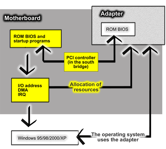 Fig. 173. Schematic overview of Plug and
Play.
Fig. 173. Schematic overview of Plug and
Play.
ESCD
The ESCD store is used to save adapter configuration information. This means the motherboard doesnt have to go through the whole plug and play operation at each startup information about the PCs configuration can be read from the CMOS storage.
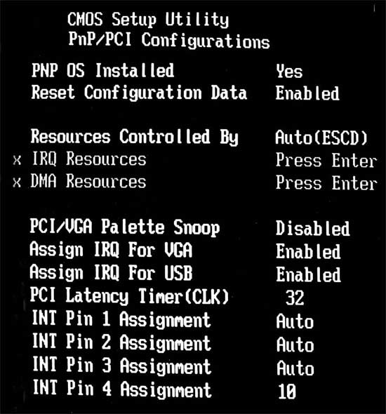 Fig. 174. Using the CMOS setup program, the user can directly allocate resources
for PCI adapters.
Fig. 174. Using the CMOS setup program, the user can directly allocate resources
for PCI adapters.
See the devices during startup
All I/O devices have small, built-in registers (in ROM circuits), which contain various information. The registers can, for example, describe the nature of the device (e.g. a network card, video card or SCSI controller, etc.) and the manufacturer. You can see this information for yourself during PC startup, when the devices are configured:
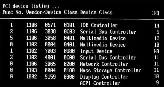 Fig. 175. The PCI devices identify themselves during startup as they are
configured.
Fig. 175. The PCI devices identify themselves during startup as they are
configured.
PCI Express development
In
This new I/O bus will be extremely scalable, as it works with a large number of channels (X1, X2, X16 etc.), each of which has a bandwidth of about 250 MB/second in both directions, simultaneously.
The standard plans for the use of plug-in cards and devices in various categories, with varying bandwidths and power consumption. A 16X video card, for example, will totally be able to pull about 8 GB/sec.
PCI Express is based on a serial architecture, making it possible to develop smaller and cheaper devices with many fewer pins. The new I/O bus will initially co-exist with the PCI interface, as we se it in the motherboards with Intel i900-series chip sets. But the goal is that PCI Express should replace both PCI and AGP.