Copyright Michael Karbo and ELI Aps., Denmark, Europe.
Chapter 42. I/O and The south bridge
We have now looked at the various I/O buses, and the chipsets south bridge plays the central role in the transfer of data on these buses. But, as mentioned before, the south bridge is assisted by a small Super I/O controller. Let me describe it briefly.
Functions of the south bridge
The south bridge is a chip on the motherboard. If we want to look at one of the latest models, we could take the south bridge from Intels 915 chipset, which is designed for motherboards with Pentium 4 processors.
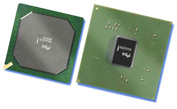
A peek at the chips specifications reveals that it contains the following components and functions:
|
Component |
Description |
|
DMI |
Direct Media Interface is the connection to the memory with a bandwidth of max 2 GB/sec. |
|
PCI Express |
Hi-speed bus for I/O adapters |
|
PCI ports |
Standard I/O bus. |
|
Serial ATA |
Controller for up to four SATA hard disks |
|
Matrix Storage |
Advanced Host Controller Interface for RAID 0 and 1 on the same drives. Including support for Native Command Queuing and hot plug drive swaps. |
|
Ultra ATA/100 |
Controller for PATA devices like hard disks, DVD- and CD-drives. |
|
USB ports |
Hi-speed USB 2.0 ports. |
|
7.1 channel audio |
Option for integrated sound device with surround, Dolby Digital and DTS. |
|
AC97 modem |
Integrated modem. |
|
Ethernet |
Integrated
10/100 Mbs network |
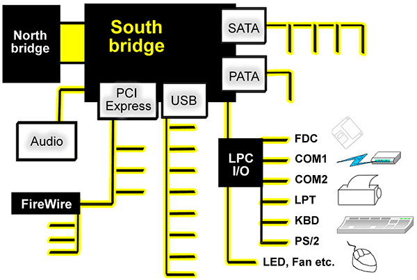
Figure 192. Selected functions in a modern south bridge.
But a number of traditional controllers for the floppy disk drive etc. are missing. These can be placed in the Super I/O controller.
Super I/O
The so-called Super I/O controller is found on all motherboards. It is a helper chip, which looks after a number of the less demanding controller functions for the south bridge.
The tasks of the Super I/O controller are quite well-defined: it is therefore fine to use a mass-produced, standard chip, which can be used on virtually any motherboard. This helps keep prices down, and these Super I/O controllers come from companies like Winbond and ITE.
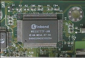
The super I/O controller is connected to the south bridge using a special low-speed bus, and this architecture is called LPC (Low Pin Count). The chip is a 128-pin chip containing these components:
|
Controller |
Description |
|
FDC |
82077-compatible floppy disk controller |
|
UART |
Serial port, 16550-compatible controller, including IrDA (infrared) |
|
LPT |
Parallel printer port |
|
Game |
For a joystick |
|
KBD |
8042-compatible keyboard controller |
|
PS/2 |
Mouse port |
|
LED |
Controls the small LEDs in the cabinet |
|
Fan |
Controls the fan |
Figure 194. Functions which the Super I/O chip typically takes care of.
You will find many different layouts of the motherboard. The south bridge may be connected to other controller chips. This could be:
It is up to the individual motherboard manufacturers to decide how they will use the chipset. The south bridge offers loads of facilities which can be implemented if desired.
For example, some south bridges have built-in primitive sound devices (based on the AC-97 standard). This uses the CPU to process sound. On some motherboards this functionality will be put to use, while other manufacturers will choose to integrate a real sound chip from, for example, Creative.
In any case, some users will choose to install a separate sound card with even more functionality regardless of what sound features the motherboard offers.
The serial and parallel ports
The serial and parallel ports are included in the I/O system, and their controller is located in the Super I/O controller.
The PC is equipped with at least one (usually two) asynchronous serial ports. These are the male connectors on the back of the PC, which have either 9 or 25 pins, of which often only 3-4 are used for serial transmission.
The parallel port is also called the printer port, because that is what it is normally used for. The printer connector on the back of the PC is a 25-pin female connector.
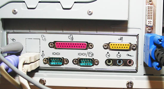
The ports are also called COM1, COM2 and LPT. These are so-called logical device names, which the PC startup program automatically allocates to these devices during startup, just as A:, C:, CON, PRN and KBD are logical names.
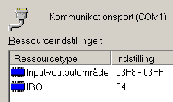
Today the serial ports and serial devices are used much less than they used to be. This is especially due to the USB bus, which can connect equivalent devices. But if you use, for example, a USB based modem, it will behave just as if it was a normal serial device. Below an ISDN adapter is installed, which is connected via USB. It creates two virtual COM ports which can be seen using the Device Manager. In this way the Internet dialup program can use the USB device in exactly the same way as if it was connected to a (physical) COM port:
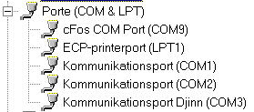
Figure 198. The COM3 and COM9 ports are actually a USB device.
Asynchronous transmission
The serial ports work using asynchronous transmission, which it might be interesting to know a little bit about.
Asynchronous transmission means that data can be transferred at irregular intervals, as you might already be familiar with from using a modem. The transmission only starts when the receiver is ready to receive. And the receiver can use unlimited time to digest the data. The opposite principle is synchronous transmission, where a shared clock controls the pace.
The irregularity means that you have to be able to work out when to send data, and when a portion of data has been sent completely. This is achieved using a protocol, which defines the packet sizes, etc., which the sender and receiver have to agree on.
When the sender has nothing to say, a stream of 1s is sent. At the start of a transmission, a 0 is sent. After this start bit, the data is sent in portions of 5, 6, 7 or 8 bits. Then follows 0, 1 or 2 so-called parity bits, which are used to perform a simple check on the transfer, and the packet is closed with 1 or 2 stop bits. The most common standard is 8 data bits, no parity bit and 1 stop bit. This system is often called 8/N/1.
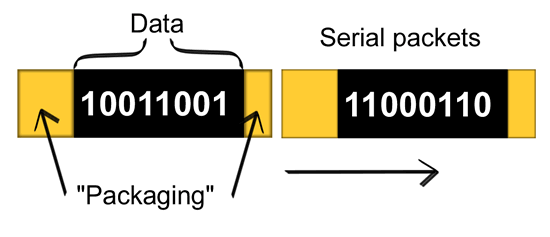
The necessary packaging of data into portions for serial transmission takes place in the UART chip, which is part of the Super I/O controller.
UART stands for Universal Asynchronous Receiver/Transmitter. The UART chip converts the data stream between the parallel I/O bus and the serial connection. Bytes from the I/O bus have to be chopped up into series of bits and framed with stop bits, etc., and this takes place in the UART.
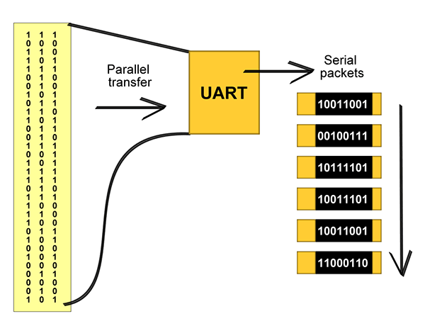
Figure 200. The UART controller repackages data in order to be able to perform a serial transfer.