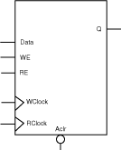

On-chip RAM
Parameterized word length and depth
Dual-port synchronous RAM architecture
Dual-port synchronous FIFO (write and read clocks are separated) with no static flag logic
Global reset of FIFO address pointers
Behavioral simulation model in VHDL and Verilog
3200DX, MX, SX, SX-A, eX
The SmartGen FIFO cores use the 3200DX and MX 32x8 or 64x4 on-chip RAM cells. SmartGen generates addresses internally using counters and token chains to address the RAM blocks (transparent to the user). Dedicated read and write address data paths are used in the FIFO architecture. The read and write operations are independent and can be performed simultaneously.
The WIDTH (word length) and DEPTH (number of words) have continuous values but the choice of WIDTH limits the choice of DEPTH and vice versa.
The asynchronous clear signal, Aclr, can be active low or active high (low is the default option and is the preferred use for all synchronous elements in the two supported families). When the asynchronous clear is active, all internal registers used to determine the current FIFO read and write addresses (counters and token chains) are reset to '0'. The FIFO is now in an empty state; the RAM content is not affected. When power is first applied to the FIFO, the FIFO must be initialized with an asynchronous clear cycle to reset the internal address pointers.
The write enable WE and read enable RE signals are active high request signals for writing into and reading out of the FIFO respectively. The WE and RE signals only control the logic associated with the FIFO write and read address pointers.
When WE is asserted high, the write cycle is initiated, and Data are written into the FIFO. The design using the FIFO is responsible for handling the full and empty states of the FIFO core.
When RE is asserted high, the read cycle is initiated, and Q is read from the FIFO. The design using the FIFO is responsible for handling the full and empty states of the FIFO core.
|
Port Description |
|
Port Name |
Size |
Type |
Req/Opt |
Function |
|
Data |
WIDTH |
Input |
Req. |
Input Data |
|
WE |
1 |
Input |
Req. |
Write Enable |
|
RE |
1 |
Input |
Req. |
Read Enable |
|
WClock |
1 |
Input |
Req. |
Write clock |
|
RClock |
1 |
Input |
Req. |
Read clock |
|
Q |
WIDTH |
Output |
Req. |
Output Data |
|
Parameter Description |
|
Parameter |
Value |
Function |
|
WIDTH |
Width |
Word length of Data and Q |
|
DEPTH |
Depth |
Number of FIFO words |
|
WCLK_EDGE |
RISE FALL |
WClock can be rising or falling |
|
RCLK_EDGE |
RISE FALL |
RClock can be rising falling |
|
Implementation Parameters - MX/DX |
|
Parameter |
Value |
Description |
|
LPMTYPE |
LPM_FIFO_DQ |
Generic FIFO category |
|
LPM_HINT |
SFIFO |
Synchronous FIFO with no flags |
|
Implementation Parameters - SX/SX-A |
|
Parameter |
Value |
Description |
|
LPM_HINT |
SFIFOSX |
Synchronous FIFO with no flags |
|
Fan-in Parameters |
|
Parameter |
Value |
Description |
|
RAMFANIN |
AUTO MANUAL |
See Fan-In Control |
Timing waveforms for this core are available in the SmartGen Cores Reference Guide. The reference guide is located in the Designer\doc directory on the hard drive where you installed your Actel Libero IDE or Designer software.