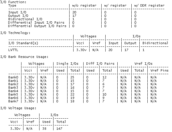
The I/O Bank report provides information about the I/O functionality, I/O technologies, I/O banks and I/O voltages.
To generate the I/O bank report:
From the Tools menu, choose Reports. This displays the Report Types dialog box.
Select IOBank in the Report types and click OK. The IOBank report opens in a separate window. You can save or print the report.
The following section shows an excerpt from the I/O Bank report:

This section of the report indicates the total number of regular input, output, and bidirectional signals. This also shows the differential input and output in the design. The I/O categories are: regular I/Os, registered I/Os or DDR I/Os in the current design.
This section of the report specifies the VCCI and VREF voltage requirements for each I/O standard and the number of user I/Os per I/O standards used in the current design.
Note: For voltage referenced I/O standards, input and bidirectional I/Os require both a VCCI and a VREF power supply whereas output I/Os only require a VCCI power supply. This is why these two categories are shown separately in this section.
This section of the report specifies the following I/O bank characteristics:
VCCI and VREF voltages assigned for each bank.
Total number of single-ended I/Os available and used for each bank.
Total number of differential I/O pairs available and used for each bank.
Total number of VREF pins assigned for each bank. This information is only relevant if a bank has been assigned a VREF voltage.
Total number of voltage referenced I/Os available and used for each bank. Voltage referenced I/Os are available only if VREF pins have been assigned.
This section of the report indicates the current design voltage requirements.
For each VCCI and VCCI/VREF user I/O demand in the current design, this table reports the total number of bonded I/Os available on the device that satisfy this demand.
Note: For an I/O bank assignment (VCCI and VREF assignment) to be valid for the current design, the I/O voltage table must show no violation. Violations are indicated with an asterisk ("*") when the number of user I/Os that need a given VCCI or VCCI/VREF assignment is less than the total number of bonded I/Os that can satisfy this demand.