Virtex
Series FPGAs
Redefining
the FPGA
Within one year of launching the original Virtex
series, Xilinx has raised the bar yet again by introducing the next generation
1.8-volt Virtex-E family that enhances all aspects of the Virtex attributes.
Fabricated on a leading edge 0.18 um, six-layer metal silicon process,
the Virtex-E family has significantly increased both performance and density,
while providing a high-performance system level feature set that further
addresses the bandwidth requirements of the next generation data communication
and DSP applications. The advanced high-performance feature set of the
Virtex series includes:
-
Densities ranging from 50,000 to 3.2 million system gates
-
Support for 20 I/O standards, including three differential signaling standards
-
Over 311 Mbps single-ended I/O performance
-
622 Mbps differential I/O performance
-
Up to 832 Kbits of internal True Dual-Port(TM) BlockRAM
-
8 DLLs for 311+ MHz clock management
-
Up to 804 single-ended I/Os or 344 differential I/O pairs
-
Direct interfacing to high performance memory devices
-
A complete package offering including high pin count, high thermal dissipation,
and low-cost packages
Since it is fully supported by Xilinx(TM) Alliance
Series(TM) and Foundation Series(TM)
software, as well as all of the EDA tools from Xilinx Alliance partners,
the Virtex series is a complete solution ready to meet the challenges of
next generation designs. The available software also includes the built-in
CORE Generator(TM) tool with a variety of web downloadable
Smart-IP(TM) BaseBlox(TM) cores.
The Virtex solution helps system designers quickly create very complex
designs with guaranteed results.
The First FPGA Solution to Deliver Over 100 Gigabits
Per Second (Gbps) I/O Bandwidth
With the growth of the Internet fueling the need for higher data transfer
rate, system designers are constantly challenged to maximize the bandwidth
of their data communication systems. Bandwidth is a key differentiator
for many end products. The fact that computing architectures are now measured
in million of instructions per second (MIPS) and data communication systems
are measured in gigabits per second (Gbps) further underscores the importance
of bandwidth. The Virtex-E family couples advanced DLLs with high-performance
SelectI/O+(TM) and SelectLink(TM)
technologies that deliver I/O performance at over 311 Megabits per second
(Mbps). This enables Virtex-E family to support high performance systems
that require bandwidth of over 100 Gbps.
SelectI/O+ Technology
-
20 single-ended and differential signaling standards are supported by all
I/Os
-
Up to 344 pairs of differential I/O pairs supporting LVPECL, Bus LVDS,
and LVDS
-
Up to 804 single-ended I/Os at over 311 Mbps each
-
622 Mbps LVDS and LVPECL performance
-
Simultaneous support of multiple voltages by all I/Os (1.8, 2.5, 3.3, and
5*** volts)
|
SelectLink Technology
-
Double-Data Rate (DDR) Virtex-E to Virtex-E link
-
Bandwidth of 300+ Mbps per pin
-
19.2 Gbps with 64-bit data-path using SSTL2
-
Built-in FIFOs and flow-control
-
Web-based HDL generation methodology
-
User enters internal and external bus-widths, FIFO resources, and I/O standard
selection
-
HDL (Verilog/VHDL) modules generated in seconds
|
Table 1. I/O Standards Supported by Virtex-E Family
| Standard |
Typical Application |
| LVTTL |
3.3 V General Purpose |
| LVCMOS2 |
2.5 V General Purpose |
| LVCMOS18** |
1.8 V General Purpose |
| PCI33_5* PCI66_5* |
33/66 MHz 5 V PCI Backplane |
| PCI33_3, PCI66_3 |
33/66 MHz 3.3 V PCI Backplane |
| SSTL2 (I,II), SSTL3(I,II), CTT |
SDRAM, DDR SRAM |
| HSTL(I,III,IV) |
SRAM, DDR SDRAM, Backplanes |
| GTL, GTL+, AGP |
Backplanes, Microprocessor Interfacing |
| LVDS** |
Point-to-Point Backplanes, High Noise Immunity |
| BLVDS** |
Bus LVDS Backplanes, High Noise Immunity, Bus Architecture
Backplanes |
| LVPECL** |
High Performance Clocking, Backplanes, Differential 100MHz+
Clocking, Optical Transceiver, High Speed Networking, and Mixed-Signal
Interfacing |
| 5 V TTL***( 4mA Iol ) |
Legacy 5V TTL Interfacing |
* Supported by Virtrex family only
** Supported by Virtex-E family only
*** Requires 100 Ohm external resistor for Virtex-E
family
The First FPGA Solution To Deliver Complete High-Performance
Differential Signaling Support
As the need for higher bandwidth continues to accelerate, system designers
are turning to differential signaling as the mechanism of choice to satisfy
high bandwidth requirements while reducing power, increasing noise immunity,
and decreasing EMI emissions. The Virtex-E family delivers the industry's
highest bandwidth and the most flexible differential signaling solution.
The selectI/O+ technology offers direct interfacing to Low Voltage Positive
Emitter Coupled Logic (LVPECL), Low Voltage Differential Signaling (LVDS),
and Bus LVDS (BLVDS) differential I/O standards. The Virtex-E family offers
a hierarchy of differential support, including up to 36 pairs for LVDS
and LVPECL at 622 Mbps, and up to 344 differential pairs at over 311 Mbps.
High performance and flexibility of the differential solution enables the
Virtex-E family to provide multiple 10 Gbps ports while maintaining high
signal integrity. Unlike other PLD solutions, all Virtex-E differential
I/Os support input, output, and I/O signaling, providing system designers
with the unparalleled flexibility to create interfaces to industry standard
differential signaling devices. In addition, Virtex-E BLVDS capability
can also support multiple configurations including standard Point-to-Point,
Multi-Point data distribution and Multi-Drop bus configurations. This feature
allows designers to customize their high-performance backplane applications
while maximizing overall bandwidth.
Table 2. Virtex-E Family LVDS and BLVDS Support
| Configuration/ Differential Signaling |
LVDS |
Bus LVDS |
| Point-to-Point |
Yes |
Yes |
| Multi-Drop |
No |
Yes |
| Multi-Point |
No |
Yes |
Table 3. Virtex-E Aggregate Bandwidth Summary
| I/O Standard |
Type |
Number of Device I/O Pins
|
|
1
|
2
|
32
|
72
|
688
|
804
|
| SSTL |
Single Ended |
311 Mbps |
622 Mbps |
10 Gbps |
22 Gbps |
214 Gbps |
250 Gbps |
| HSTL |
Single Ended |
311 Mbps |
622 Mbps |
10 Gbps |
22 Gbps |
214 Gbps |
250 Gbps |
| GTL+ |
Single Ended |
311 Mbps |
622 Mbps |
10 Gbps |
22 Gbps |
214 Gbps |
250 Gbps |
| LVDS |
Differential |
n/a |
622 Mbps |
10 Gbps |
22 Gbps |
107 Gbps |
n/a |
| LVPECL |
Differential |
n/a |
622 Mbps |
10 Gbps |
22 Gbps |
107 Gbps |
n/a |
| Bus LVDS |
Differential |
n/a |
311 Mbps |
5 Gbps |
11 Gbps |
107 Gbps |
n/a |
The First FPGA To Provide High-Performance Clocking
LVPECL clocking becomes an essential requirement as FPGA system clock
frequencies exceed 100 MHz. The Virtex-E device supports high-performance
LVPECL clock inputs for global and local clocking with frequencies in excess
of 300 MHz. In addition, through the use of multiple DLLs and SelectI/O+
technology, Virtex-E devices enable zero-delay conversion of precise LVPECL
clocks into virtually any required I/O standard. These features allow Virtex-E
FPGAs to become an integral part of high-performance board-level clock
distribution strategies.
The First FPGA To Deliver Terabits Per Second (Tbps)
Memory Bandwidth
The Virtex series offers a hierarchy of memory resources employing the
SelectRAM+ technology. The Virtex series delivers up to 208 blocks of synchronous
4 Kbits True Dual-Port(TM) RAM (832-Kb total) - twice
the memory resources of any other programmable logic family available today.
With internal Block RAM performance that reaches 250 MHz, coupled with
True Dual-Port capability, the Virtex series can deliver up to 1.66 Tbps
of memory bandwidth, which is ideal for buffering multiple high-performance
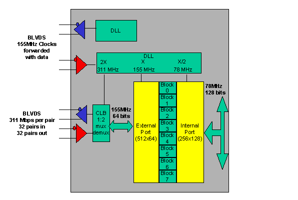
data ports. The following diagram illustrates how Virtex-E devices meet
the bandwidth requirement for an OC-192 application.
The Virtex series also offers over 1Mbits of distributed RAM, which
is ideal for high-speed data processing applications. Furthermore, with
the enhanced performance provided by the SelectI/O+ and DLL capabilities
of the Virtex-E family, the Virtex series can directly interface to high
performance memory devices including 200 MHz ZBT SRAMs, 266 MHz DDR SDRAMs,
and future QDR SRAMs. The precise 50/50 duty cycle generation of DLLs makes
the Virtex series ideally suited for high-performance DDR applications.
|
Virtex SelectRAM+ Memory Hierarchy
|
| Distributed SelectRAM+ Memory |
|
Block SelectRAM+ Memory |
|
High-Speed External Memory Interface |
| The vast array of configurable logic blocks
(CLBs) are each configurable as a 16x1, 16x2, 16x3, 16x4, 32x1 or 32x2
synchronous RAM, or as a 16x1, 16x2 or 32x1 dual-port synchronous RAM |
|
Dedicated blocks of on-chip 4 Kbit True Dual-Port
synchronous RAM for critical high-bandwidth memory, configurable as 4Kx1,
2Kx2, 1Kx4, 512x8, and 256x16 |
|
Direct interface to:


- 133 MHz SDRAM

- 200 MHz ZBT SRAM

- 266 MHz DDR SDRAM

- Future QDR SRAM
|
The Virtex Series Solution:
Leading-Edge Software and Intellectual Property (IP) Support
The Virtex architecture was designed in conjunction with our synthesis
partners in order to assure maximum performance, predictability, and simplified
integration of intellectual property. The Xilinx solution includes:
-
Complete Virtex series support in Alliance Series and Foundation Series
software, both of which feature powerful implementation tools to maximize
performance while enhancing productivity
-
Optimized place and route algorithms that provide a 50% reduction in compile
time as compared to the previous software release
-
Team-based design environment, through Xilinx Internet Team Design (Xilinx
iTD(TM)) tool,that increases productivity for multi-module
designs
-
Support for third party signal analysis tools which ensures clean signal
integrity (Alliance Series only)
-
Smart-IP technology and CORE Generator tools that enable high design productivity
-
BaseBlox cores that have been highly optimized for performance and utilization
-
The Real-PCI(TM) 64/66 and 32/33 LogiCORE(TM)
solutions that are fully PCI compliant
-
A variety of AllianceCORE(TM) products which span
a breadth of applications in communications, networking, video and image
processing, computing, and other market segments
Virtex 2.5 Volt Family
| Feature/Product |
XCV50 |
XCV100 |
XCV150 |
XCV200 |
XCV300 |
XCV400 |
XCV600 |
XCV800 |
XCV1000 |
| CLB
Array (Row x Col.) |
16 x 24
|
20 x 30
|
24 x 36
|
28 x 42
|
32 x 48
|
40 x 60
|
48 x 72
|
56 x 84
|
64 x 96
|
| Logic
Cells |
1,728
|
2,700
|
3,888
|
5,292
|
6,912
|
10,800
|
15,552
|
21,168
|
27,648
|
| System
Gates |
57,906
|
108,904
|
164,674
|
236,666
|
322,970
|
468,252
|
661,111
|
888,439
|
1,124,022
|
| Max.
Block RAM Bits |
32,768
|
40,960
|
49,152
|
57,344
|
65,536
|
81,920
|
98,304
|
114,688
|
131,072
|
| Max.
Distributed RAM Bits |
24,576
|
38,400
|
55,296
|
75,264
|
98,304
|
153,600
|
221,184
|
301,056
|
393,216
|
| Delay
Locked Loops (DLLs) |
4
|
4
|
4
|
4
|
4
|
4
|
4
|
4
|
4
|
| I/O
Standards Supported |
17
|
17
|
17
|
17
|
17
|
17
|
17
|
17
|
17
|
| Speed
Grades |
4, 5, 6
|
4, 5, 6
|
4, 5, 6
|
4, 5, 6
|
4, 5, 6
|
4, 5, 6
|
4, 5, 6
|
4, 5, 6
|
4, 5, 6
|
| Max.
Avail. User I/O |
180
|
180
|
260
|
284
|
316
|
404
|
512
|
512
|
512
|
| CS144 (12mm x 12mm) |
I/O |
94
|
94
|
|
|
|
|
|
|
|
| TQ144 (20mm x 20mm) |
I/O |
98
|
98
|
|
|
|
|
|
|
|
| PQ240/HQ240 (32mm x
32mm) |
I/O |
166
|
166
|
166
|
166
|
166
|
166
|
166
|
166
|
|
| BG256 (27mm x 27mm) |
I/O |
180
|
180
|
180
|
180
|
|
|
|
|
|
| BG352 (35mm x 35mm) |
I/O |
|
|
260
|
260
|
260
|
|
|
|
|
| BG432 (40mm x 40mm) |
I/O |
|
|
|
|
316
|
316
|
316
|
316
|
|
| BG560 (42.5mm x 42.5mm) |
I/O |
|
|
|
|
|
404
|
404
|
404
|
404
|
| FG256 (17mm x 17mm) |
I/O |
176
|
176
|
176
|
176
|
|
|
|
|
|
| FG456 (23mm x 23mm) |
I/O |
|
|
260
|
284
|
312
|
|
|
|
|
| FG676 (27mm x 27mm) |
I/O |
|
|
|
|
|
404
|
444
|
444
|
|
| FG680 (40mm x 40mm) |
I/O |
|
|
|
|
|
|
512
|
512
|
512
|
Virtex-E 1.8 Volt Family (Table 1 of 2)
| Feature/Product |
XCV50E |
XCV100E |
XCV200E |
XCV300E |
XCV400E |
XCV600E |
| CLB
Array (Row x Col.) |
16 x 24
|
20 x 30
|
28 x 42
|
32 x 48
|
40 x 60
|
48 x 72
|
| Logic
Cells |
1,728
|
2,700
|
5,292
|
6,912
|
10,800
|
15,552
|
| System
Gates |
71,693
|
128,236
|
306,393
|
411,955
|
569,952
|
985,882
|
| Max.
Block RAM Bits |
65,536
|
81,920
|
114,688
|
131,072
|
163,840
|
294,912
|
| Max.
Distributed RAM Bits |
24,576
|
38,400
|
75,264
|
98,304
|
153,600
|
221,184
|
| Delay
Locked Loops (DLLs) |
8
|
8
|
8
|
8
|
8
|
8
|
| I/O
Standards Supported |
20
|
20
|
20
|
20
|
20
|
20
|
| Speed
Grades |
6, 7, 8
|
6, 7, 8
|
6, 7, 8
|
6, 7, 8
|
6, 7, 8
|
6, 7, 8
|
| Max.
Avail. User I/O |
176
|
176
|
284
|
316
|
404
|
512
|
| Package |
Differential Pairs |
|
| CS144 (12mm x 12mm) |
30
|
I/O
|
94
|
94
|
94
|
|
|
|
| PQ240/HQ240 (32mm x
32mm) |
64
|
I/O
|
158
|
158
|
158
|
158
|
158
|
158
|
| BG432 (40mm x 40mm) |
137
|
I/O
|
|
|
|
316
|
316
|
316
|
| BG560 (42.5mm x 42.5mm) |
183
|
I/O
|
|
|
|
|
|
|
| FG256 (17mm x 17mm) |
83
|
I/O
|
176
|
176
|
176
|
176
|
|
|
| FG456 (23mm x 23mm) |
119
|
I/O
|
|
|
284
|
312
|
|
|
| FG676 (27mm x 27mm) |
183
|
I/O
|
|
|
|
|
404
|
444
|
| FG680 (40mm x 40mm) |
247
|
I/O
|
|
|
|
|
|
512
|
| FG860 (42.5mm x 42.55mm) |
281
|
I/O
|
|
|
|
|
|
|
| FG900 (31mm x 31mm) |
260
|
I/O
|
|
|
|
|
|
512
|
| FG1156(35mm x 35mm) |
344
|
I/O
|
|
|
|
|
|
|
Virtex-E 1.8 Volt Family (Table 2of 2)
| Feature/Product |
XCV1000E |
XCV1600E |
XCV2000E |
XCV2600E |
XCV3200E |
| CLB
Array (Row x Col.) |
64 x 96
|
72 x 108
|
80 x 120
|
92 x 138
|
104 x 156
|
| Logic
Cells |
27,648
|
34,992
|
43,200
|
57,132
|
73,008
|
| System
Gates |
1,569,178
|
2,188,742
|
2,541,952
|
3,263,755
|
4,074,387
|
| Max.
Block RAM Bits |
393,216
|
589,824
|
655,360
|
749,568
|
851,968
|
| Max.
Distributed RAM Bits |
393,216
|
497,664
|
614,400
|
812,544
|
1,038,336
|
| Delay
Locked Loops (DLLs) |
8
|
8
|
8
|
8
|
8
|
| I/O
Standards Supported |
20
|
20
|
20
|
20
|
20
|
| Speed
Grades |
6, 7, 8
|
6, 7, 8
|
6, 7, 8
|
6,7,8
|
6,7,8
|
| Max.
Avail. User I/O |
660
|
724
|
804
|
804
|
804
|
| Package |
Differential Pairs |
|
| CS144 (12mm x 12mm) |
30
|
I/O
|
|
|
|
|
|
| PQ240/HQ240 (32mm x
32mm) |
64
|
I/O
|
158
|
|
|
|
|
| BG432 (40mm x 40mm) |
137
|
I/O
|
|
|
|
|
|
| BG560 (42.5mm x 42.5mm) |
183
|
I/O
|
404
|
404
|
404
|
1 |
1 |
| FG256 (17mm x 17mm) |
83
|
I/O
|
|
|
|
|
|
| FG456 (23mm x 23mm) |
119
|
I/O
|
|
|
|
|
|
| FG676 (27mm x 27mm) |
183
|
I/O
|
|
|
|
|
|
| FG680 (40mm x 40mm) |
247
|
I/O
|
512
|
512
|
512
|
|
|
| FG860 (42.5mm x 42.55mm) |
281
|
I/O
|
660
|
660
|
660
|
1 |
1 |
| FG900 (31mm x 31mm) |
260
|
I/O
|
660
|
700
|
|
|
|
| FG1156(35mm x 35mm) |
344
|
I/O
|
660
|
724
|
804
|
804
|
804
|
Summary
The revolutionary 2.5-volt Virtex family of FPGAs broke new density
and performance barriers by expanding the traditional usage of the programmable
logic, delivering the first FPGA platform that truly addressed system-level
design challenges. With the introduction of the next generation 1.8-volt
Virtex-E family, Xilinx has taken FPGA performance to the next level, thereby
providing a compelling alternative to ASIC solutions. Virtex series consists
of two high-performance FPGA families that range in density from 50,000
to 3,200,000 system gates with up to 622 Mbps I/O performance. The Virtex
series features advanced DLLs for high-performance clock management, a
hierarchy of memory resources, and I/Os capable of simultaneously interfacing
to twenty voltages and signaling standards. The Virtex series solution
combines maximum I/O and memory bandwidths with leading-edge software and
IP support in order to deliver a solution that best addresses the bandwidth,
cost and time-to-market challenges of the next generation data communication
and DSP applications. |