Functions
Interfacing the processor to the memory modules requires at least two critical
abilities - electrical compatibility and speed. Electrical compatibility
between the processor and chosen memories - FLASH EPROM, SRAM or DRAM is
basically resolved by using Xilinx 3.3 volt PLD technologies. Available
in both SpartanXL FPGA and XC9500XL
CPLDs, the ability to freely connect 5V and 3.3V processors and memories
is easily resolved.
For the choice of PLDs to achieve the DRAM interface, either a SpartanXL
FPGA or a XC9500XL CPLD could be used
to create a mixed 3.3V/5V DRAM interface. The SpartanXL would consume less
power than the XC9500XL, however the XC9500XL can typically create a faster
DRAM interface if power is not the issue.
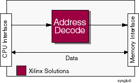
For the SRAM and FLASH EPROM interfaces, users frequently want the simplicity
of a CPLD for its wide address decode capability and pin retention architecture.
Advantages
Both SpartanXL and XC9500XL
devices can be used in a memory interface application such as this. SpartanXL
has the advantage of lower operating and standby power while the XC9500XL
will offer faster DRAM interface capability and wider decode capability
for SRAM, FLASH, or EPROM. Both options are substantially lower priced
than competitive alternatives. |