Introduction
This application note illustrates the use of Spartan devices in an Integrated
Services Digital Network (ISDN) modem. In this application the Spartan
device is used to implement the complex system level glue logic required
for the modem's PCMCIA interface. The Spartan device provides host
interface functions for an ISDN U interface controller and includes HDLC
framing. The design example shows how cost effective a Spartan device
can be in these applications.
While the design is targeted at solving a specific problem, interfacing an ISDN
U interface transceiver to PCMCIA, it illustrates solutions to a number of general
technical issues. These include handling HDLC data streams and interfacing
to Time Division Multiplexed (TDM) serial buses. This document assumes that
the reader is familiar with ISDN and PCMCIA technologies.
Overview
A key design objective for this application was the creation of a solution with
the lowest possible cost. In this case the target was a semiconductor bill
of materials for the PCMCIA interface that is significantly less than $20 in volume.
A second objective was to simplify the design effort by utilizing as much commercially
available Intellectual Property (IP) as possible.
Figure 1 gives an overview of the design. It consists
of an ISDN U-Interface transceiver, the Spartan device, and external memory.
The device that was chosen for the ISDN U-Interface in this application is a Motorola
MC145572. The U-Interface connects to the rest of the design by way of two
interfaces. The IDL interface is a five-wire TDM interface, defined by Motorola,
and carries the B and D channel data. The PCP interface is an eight-bit microprocessor
bus interface used to access the internal control and status registers of the U-Interface
transceiver.
Figure 1: Simplified ISDN Modem System Block Diagram
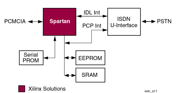 Three external memory devices are connected to the Spartan device.
A serial configuration PROM is used for device initialization. A 2Kx8 EEPROM
is used to store the PCMCIA CIS data structure. An 8Kx8 SRAM provides buffering
for incoming and outgoing ISDN traffic. Three external memory devices are connected to the Spartan device.
A serial configuration PROM is used for device initialization. A 2Kx8 EEPROM
is used to store the PCMCIA CIS data structure. An 8Kx8 SRAM provides buffering
for incoming and outgoing ISDN traffic.
Before we examine the functions implemented in the Spartan device, let's
get a overview of the device that was chosen for the ISDN U-interface.
Motorola MC145572 ISDN U-Interface Transceiver
The U-Interface transceiver chosen for this design is the Motorola MC145572.
The functions performed by this device can be summarized as follows:
- Adaptive equalization
- Data and clock recovery
- Echo cancellation
- Physical layer framing
In short, it implements all of the physical layer signal processing functions
needed to interface to the wire. Figure 2 illustrates the
functional blocks that make up this device.
Figure 2: MC145572 Block Diagram
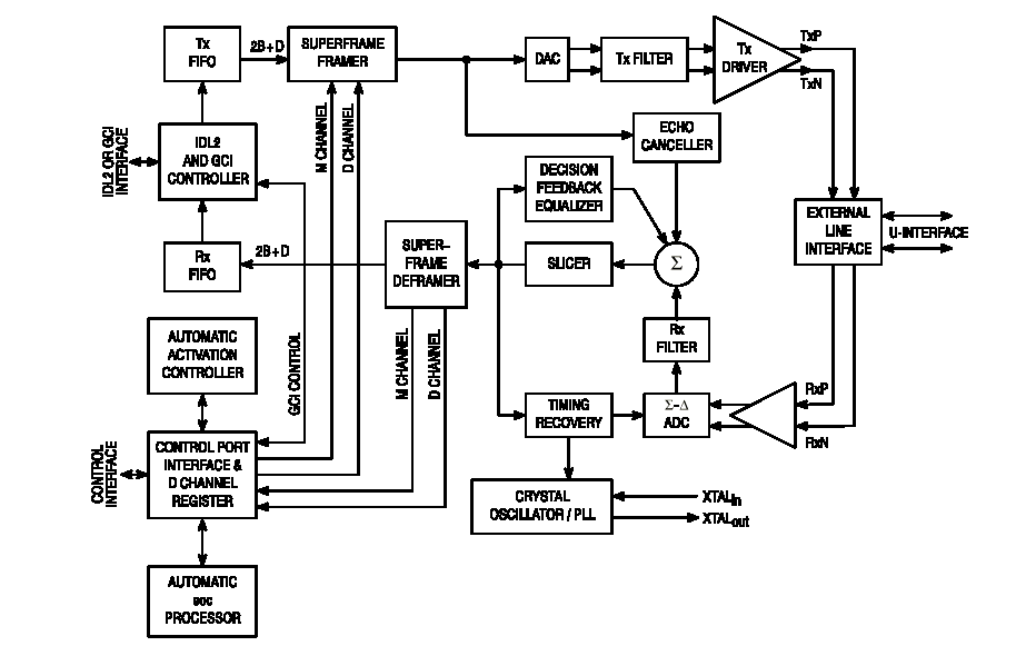 Figure Courtesy Motorola Figure Courtesy Motorola
The MC145572 includes three interfaces: the external line interface is coupled
to the twisted pair to implement ISDN U-Interface, a serial interface for transferring
ISDN data streams, and a control port used to configure the transceiver.
The control port can be configured for either serial or parallel modes of operation.
In this application the Parallel Control Port (PCP) mode is used. In this mode
the interface can be connected directly to the data bus on a standard eight bit microprocessor.
The ISDN 2B+D data is transferred over a TDM interface that can be configured
for several operating modes. The mode of operation chosen for this application
is IDL2 master, short frame master mode, with eight bit data. Figure
3 shows how the data from the two B channels and the D channel is transferred
across the IDL2 interface when configured for this mode.
Figure 3: IDL2 Timing
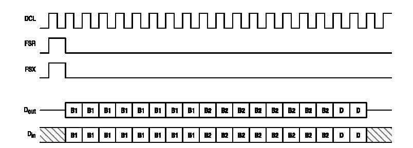
Figure Courtesy Motorola
Interface Architecture
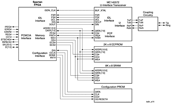
Figure 4 illustrates how all of this fits together.
Sitting in the middle of the interface, the Spartan device is truly the glue that
pulls the whole thing together. A common eight-bit data bus is used to connect
the Spartan device to the MC145572 PCP interface, the EEPROM, and the SRAM.
Figure 4: ISDN Modem Detailed System Block Diagram
Spartan Device Implementation
Figure 5 shows the architecture implemented in the Spartan
device for this application. It consists of five major functional blocks:
- PCMCIA Interface
- Memory Controller and Buffer Manager
- IDL Multiplexing and Demultiplexing
- HDLC In functions
- HDLC Out functions
Figure 5: FPGA Logic Block Diagram
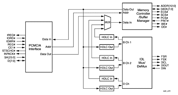
The IDL Mux/Demux block multiplexes traffic from the 2B+D channels over the IDL
interface using the frame format illustrated in Figure 3.
Incoming frame data is demultiplexed into the three channels and forwarded to the
HDLC In blocks. The block is implemented as a state machine which performs
these functions by asserting enable signals to the HDLC In and HDLC Out blocks at
the appropriate times.
The HDLC In blocks manage the detection of Link Access Procedure D channel (LAPD)
or Point to Point Protocol (PPP) frames in the incoming bit streams and formatting
them for storage by the buffer manager. Functions performed include flag detection,
zero stripping, Frame Check Sequence (FCS) checking, and serial to parallel conversion.
These functions, except for the serial to parallel conversion, can be disabled on
the B channels when they are used for voice traffic. The block supports both
CRC-16 and CRC-32 FCSs.
The HDLC Out blocks perform the inverse function of the HDLC In blocks.
Specifically they perform parallel to serial conversion, FCS generation, bit stuffing,
and flag insertion. Like the HDLC In blocks, all functions except for the parallel
to serial conversion can be disabled on the B channels when they are used for voice
traffic.
The Memory Controller/Buffer Manager is the most complicated block in the design.
It performs three major functions:
- Arbitrating access to the three devices that are connected to the data bus: SRAM,
EEPROM and the MC145572 PCP
- Generating device control signal timing for each of the three devices
- Managing input and output queues for the three channels in the external SRAM
The Memory Controller portion of this block handles the first of these two functions,
while the Buffer Manager portion handles queue management.
The Memory Controller allocates access to the PCP interfaces and external memory
by dividing the bus bandwidth into access time slots. The 20.480000 MHz ISDN_CLK
signal is used to clock the memory controller state machine. This state machine
generates eight bus time slots, each of which is 195.3ns or 4 ISDN_CLK cycles long.
Four bus time slots are allocated for PCMCIA access to either the memory buffers
or the PCP interface. The remaining time slots are allocated for buffer manager
access to each of the six data queues. This results in available PCMCIA bandwidth
of 2.56 megabytes per second and an average access time of 293ns.
The Buffer Manager maintains six queues in the external SRAM for buffering data
to and from the three ISDN channels. Each queue is statically allocated 1 KB
of the available memory, with the remaining 2 KB of memory are unused. Each
queue is a simple FIFO, and PCMCIA access to the queue data is through three I/O
ports, and six sets of control and status registers.
The PCMCIA interface block handles decoding and handshaking functions. In
addition, the block implements the PCMCIA Function Configuration Registers (FCRs).
These eight bit registers consist of the Configuration Option Register and the Configuration
Status Register.
Spartan Device Selection
Spartan devices are available in a range of densities and packages. The
following criteria were used to select the device used in this application.
|