|
||
|
|
||
Xilinx : Support : techXclusives |
|||||||||||||||||||||||||||||||
|
|
|||||||||||||||||||||||||||||||
| techXclusives | |||||||||||||||||||||||||||||||
|
|||||||||||||||||||||||||||||||
|
|||||||||||||||||||||||||||||||
|
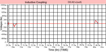
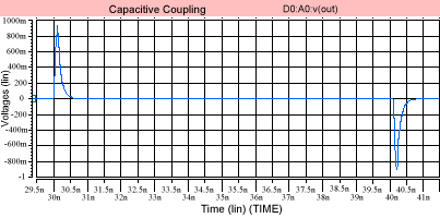
Signal Integrity (SI) engineering has become a necessary requirement for today's high-speed logic signals. Having control of cross-talk, ground bounce, ringing, noise margins, impedance matching, and decoupling is now critical to a successful design. All of these problems relate to a similar issue: Signal Integrity. SI describes the environment in which the signals must exist. It covers the various techniques and design issues that ensure signals are undistorted and do not cause problems to themselves, to other components in the system, or to other systems nearby. The Basics An electrical current in a loop generates a magnetic field. If this magnetic field is changing, it can either radiate energy by launching radio frequency waves, or it can couple to adjacent loops ("Inductive cross-talk").
The voltage on a line creates an electric field. If this electric field is changing, it radiates radio waves, or it can couple capacitively to adjacent lines ("Electrostatic cross-talk").
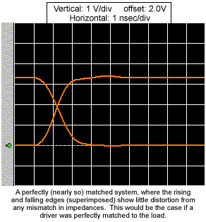
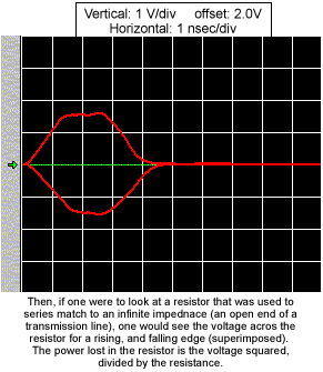
When does a line or loop radiate radio frequency waves? Basically, if the line or loop has signal energy at a frequency high enough that the line or loop represents at least a tenth of a wavelength, there will be a measurable amount of electromagnetic radiation ("Radio waves"). Why Antennas Radiate The impedance of free space is 377 ohms. If I have a perfectly matched antenna, it can be thought of as a transformer that matches the impedance of a line to the impedance of space. Wires go in, and radio waves come out. Power launched into the wires appears to go into a resistor: The voltage is in phase with the current, and no power is reflected back. A typical printed circuit board trace over ground is a transmission line whose impedance is somewhere between 35 and 100 ohms (depending on the dimensions and the insulator material). If the driving circuit has low impedance (lower than the line) and the receiving circuit has a high impedance (much higher than the line), then the line is mismatched. Energy launched from the driver will travel down to the end of the line, reflect and bounce back to the driver. At the driver, it will again be reflected and bounce back to the receiver. This process goes on until all of the energy is lost in heat, or lost through radiation into space. If the line is matched and the energy, therefore, does not bounce back and forth, radiation does not occur, as the energy is completely absorbed in the matching resistance.
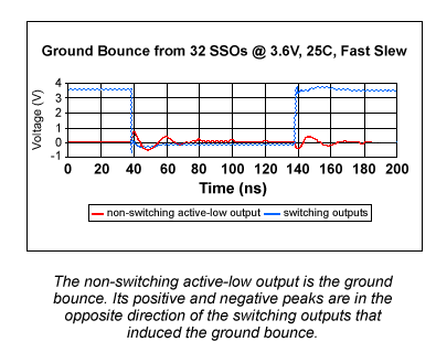
"Matched lines don't radiate" is a useful phrase to remember. Why Lines and Loops Couple If you place two lines near each other, they will couple to one another either magnetically, electrically, or both. This is because their electric and magnetic fields overlap in the near field and affect each other. The resulting cross-talk causes delay variation in the transitions, or bad signal states altogether. The solution is distance, or the addition of an "in-between" conductor to constrain the electric field. Further electrostatic shielding may not be worthwhile, as there is no good means of shielding magnetic fields besides distance. Control of the physical dimensions is absolutely necessary to control cross-talk and keep the impedance matched. How does Ground Bounce occur? If you have a number of outputs that are all capable of driving in the same direction at the same time (such as an address bus that goes from all 0's to all 1's), the resulting current from switching all of the lines simultaneously might share a common ground pin. That ground pin can rise significantly above (or below) ground due to the resultant IR drop, along with the self-inductance of that one pin. In order to prevent the resultant ground potential change from affecting other circuits nearby, or other circuits on the same integrated circuit, providing sufficient ground and power connections and their associated bypass capacitors is mandatory.
If you are driving a number of input pins and the lines are not matched, significant ringing may occur. This ringing at the receiving end might forward-bias protection diodes or structures and cause currents to be injected into the substrate (ground) or power rails. In order to minimize ground bounce, provide extra ground and supply pins and good bypassing, control the rate of rise/fall of the lines, provide impedance-matching termination, and/or minimize the number of lines. How FPGAs Help Solve Signal Integrity Problems The use of FPGAs represents an opportunity to control the signal integrity, but only if some work is done in advance of the design itself. First, a floor plan of the input and outputs should be done to make sure that the number and location of simultaneous switching outputs (SSOs) is kept within guidelines. Blocks of outputs must be kept physically distant from the critical inputs to reduce cross-talk coupling and ground bounce disturb problems. Second, unused I/O pins may be employed as virtual ground or supply pins: program them to drive a "1" or a "0" at the highest current drive strength (PCI, GTL or LVTTL 24), then tie them to PC-board power or ground. These pins will function as additional power and ground pins, keeping the ground and power bounce under control. Bypass these virtual pins just as you would a power/ground pin. Third, all inputs and outputs should be matched to the printed circuit board traces using a signal integrity analysis package; this package should model the drivers and receivers using a modeling format such as IBIS (I/O Buffer Information Specification). By adding small resistors where required, the reflections are minimized and absorbed, rather than being radiated. Another technique used in FPGAs is to control the output slew rates. If delay is not an issue, you may use SLOW output attributes to reduce cross-talk and bounce. If slew rate control is not possible, the drive strength should be programmed to a lower strength (e.g., LVTTL 2 rather than LVTTL 12). The resulting higher output resistance will absorb reflections and improve signal integrity. Through the use of certain Select I/O options, external resistors may not be necessary. Why haven't I heard of this before? Did SI suddenly jump out of nowhere? Not long ago, the highest frequencies encountered in digital circuits were below 20 MHz. To be a transmission line or an antenna at these frequencies, a structure had to be about one meter (3 feet) long. Practical circuits did not behave like transmission lines or antennas. Now that clock rates are up to 320 MHz and edge rates are a few hundred picoseconds, interconnects as short as 25 mm (1 inch) begin to look like transmission lines and antennas. Those involved in microwave radio systems design have used Signal Integrity engineering for more than 40 years. As a former radio systems designer, I say "Welcome to the real world"! Further Reading: High Speed Digital Design, A Handbook of Black Magic, Howard Johnson and Martin Graham Share your comments, questions and ideas with Austin Lesea and other interested designers at the "Signal Integrity Tips and Tricks" FORUM. |
|||||||||||||||||||||||||||||||
| |
|||||||||||||||||||||||||||||||
|
|||||
|
|
Troubleshoot | Hardware
| Software | Library
| Design | Education
| Services | | Home | Products | Support | Education | Purchase | Contact | Search | |