Parameterized models with characteristic parameter values are added to the PSpice for TI solution. The parameterized MOSFETs are: POWER_NMOS_P and POWER_PMOS_P. The parameterized diode is POWER_DIODE_P.
The parameters specified for each of these models enable you to simulate and test the model in various conditions. As a result, you can quickly observe and analyze the performance of these parameterized models in the design. For example, if you want to test multiple MOSFETs from different manufacturers, with every MOSFET having different value for RDSON and QG, then you only need to refer to the respective MOSFET datasheet and accordingly specify the parameter values in power MOSFET model. This process saves time and you need not import individual PSpice models from each manufacturer.
To place and edit a parameterized MOSFET, do the following:
- Open PSpice Part Search from one of the following:
- Click the Launch PSpice Part Search icon (
 ) from the PSpice toolbar.
 - Choose Place – PSpice Component – Search.
- Click the Launch PSpice Part Search icon (
- From the Category tab, navigate to desired PSpice part in a particular category.
For example, navigate to Discrete – MOSFET – Power MOSFET. -
From the results list, choose the parameterized N Channel Power MOSFET (
POWER_NMOS_P) or parameterized P Channel Power MOSFET (POWER_PMOS_P).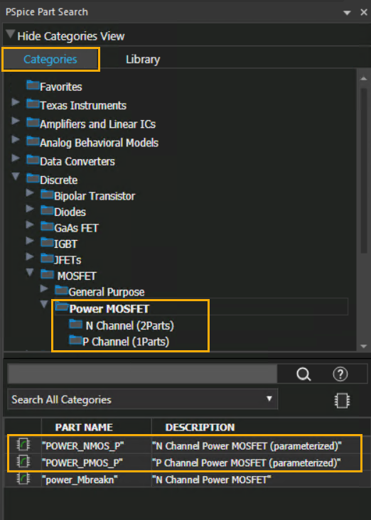
-
Right-click the selected part and select Place Symbol from the pop-up or double-click this part.
-
Move the part and click on schematic editor to place the part.
- To edit this part, use one of the following methods.
- Right-click and select Edit Properties.
- From the Edit menu choose Properties.
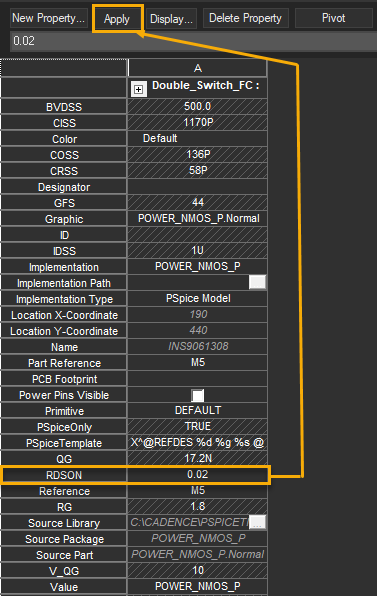
The Property Editor tab opens.
-
Select a property and modify the value as required.
For example, modify the value of
RDSONto0.02. -
Click the Apply button.
-
In the warning message that appears, click Yes.
Similarly, you can modify values of other parameters. To view the parameter details and their default value, see Parameter Description and Default Values.
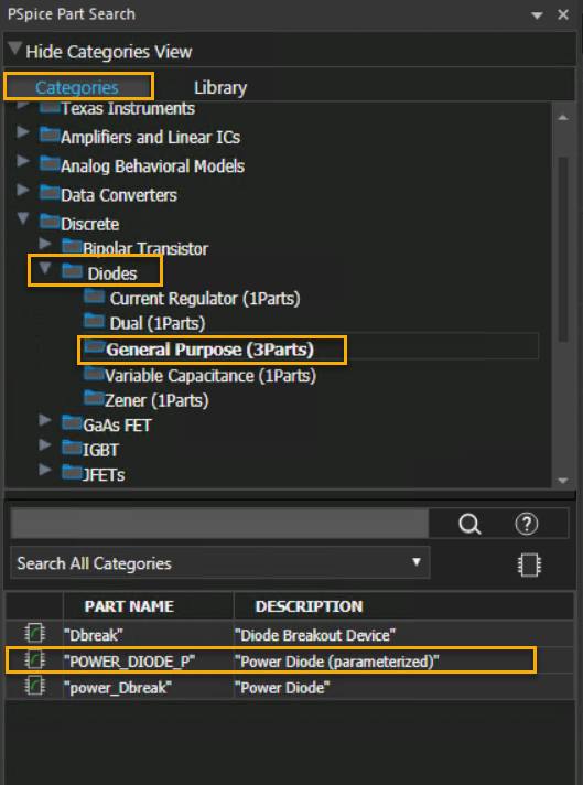
To place the parameterized power diode, navigate to Discrete – Diodes – General Purpose. Select POWER_DIODE_P as shown in the following figure. Using the steps explained above, you edit the parameters of this power diode.
If you need to frequently change the values of the model parameters, use the following method to display the required properties on the schematic editor.
- Select the parameterized MOSFET in the design.
- Open the Property Editor, using one of the following methods:
- Right-click and select Edit Properties.
- From the Edit menu choose Properties.
- In the Property Editor tab that opens, select the model property and do one of the following:
- Click the Display button.
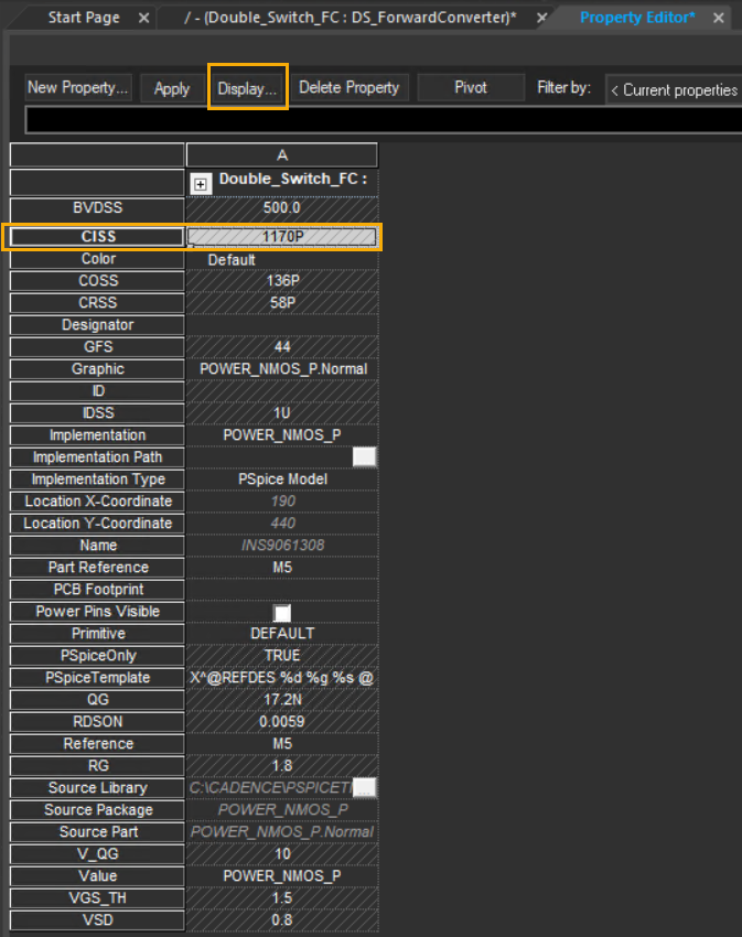
- Right-click and select Display.
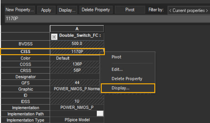
- Click the Display button.
- Select the Name and Value option.
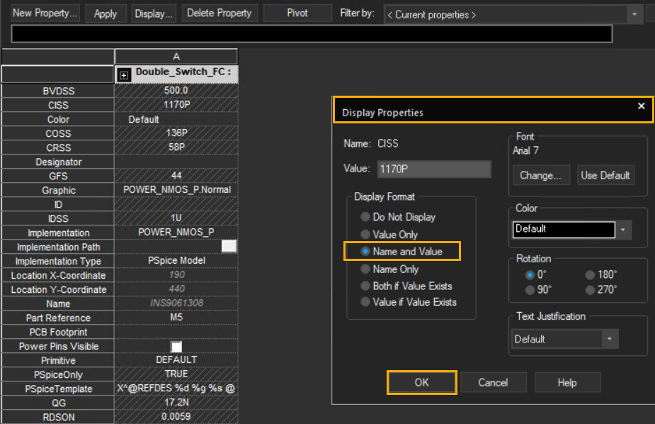
- Click OK.
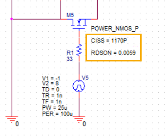
- The properties are now seen on the schematic editor.
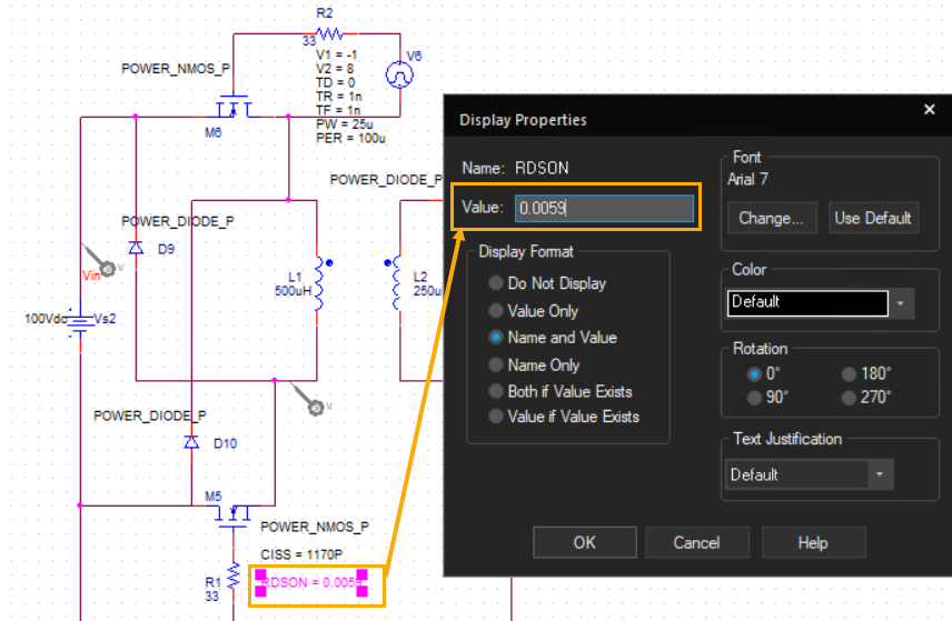
- Select and double-click any property.
The Display Properties dialog box appears. - Modify the value of the property and click OK.
Parameter Description and Default Values
The specific parameters for each of these models, their explanation, and default values are provided in the following table.
MOSFET: POWER_NMOS_P
|
S.No. |
Parameters |
Description |
Default Value (can be edited) |
Units |
|
1 |
CRSS |
Reverse transfer capacitance |
58p |
F |
|
2 |
CISS |
Input capacitance |
1170p |
F |
|
3 |
COSS |
Output capacitance |
136p |
F |
|
4 |
BVDSS |
Drain-to-source voltage (maximum voltage across MOS) |
500 |
V |
|
5 |
RDSON |
Drain-to-source on-resistance |
0.0059 |
ohm |
|
6 |
RG |
Series internal gate resistance |
1.8 |
ohm |
|
7 |
VGS_TH |
Gate-to-source threshold voltage (gate voltage at which the MOS starts conducting) |
1.5 |
V |
|
8 |
VSD |
Diode forward voltage |
0.8 |
V |
|
9 |
IDSS |
Drain-to-source leakage current |
1u |
A |
|
10 |
QG |
Total gate charge (during complete switching transient) |
17.2n |
C |
|
11 |
V_QG |
Voltage for specified total gate charge |
10 |
V |
|
12 |
GFS |
Forward trans-conductance (∆Ids/∆Vgs for fixed VDS) |
44 |
S |
MOSFET: POWER_PMOS_P
|
S.No. |
Parameters |
Description |
Default Value (can be edited) |
Units |
|
1 |
CRSS |
Reverse transfer capacitance |
52p |
F |
|
2 |
CISS |
Input capacitance |
1630p |
F |
|
3 |
COSS |
Output capacitance |
902p |
F |
|
4 |
BVDSS |
Drain-to-source voltage (maximum voltage across MOS) |
-500 |
V |
|
5 |
RDSON |
Drain-to-source on-resistance |
5.5m |
ohm |
|
6 |
RG |
Series internal gate resistance |
0.8 |
ohm |
|
7 |
VGS_TH |
Gate-to-source threshold voltage (gate voltage at which the MOS starts conducting) |
-0.9 |
V |
|
8 |
VSD |
Diode forward voltage |
-0.8 |
V |
|
9 |
IDSS |
Drain-to-source leakage current |
1u |
A |
|
10 |
QG |
Total gate charge (during complete switching transient) |
10.8n |
C |
|
11 |
V_QG |
Voltage for specified total gate charge |
-4.5 |
V |
|
12 |
GFS |
Forward trans-conductance (∆Ids/∆Vgs for fixed VDS) |
47 |
S |
Diode: POWER_DIODE_P
|
S.No. |
Parameters |
Description |
Default Value (can be edited) |
Units |
|
1 |
V_BR |
Breakdown voltage, reverse peak voltage across diode |
600 |
V |
|
2 |
I_REV_LEAK |
Reverse leakage current when diode is reverse biased |
1e-5 |
A |
|
3 |
CT_ZERO_VOLTS |
Total junction capacitance at 0V across diode |
300p |
F |
|
4 |
VJ_KNEE |
Threshold voltage (forward bias voltage required for diode to start conducting) |
0.90 |
V |
|
5 |
VJ_SPEC |
Diode voltage drop at specified forward current (IF_SPEC) |
1.6 |
V |
|
6 |
IF_SPEC |
Specified forward current |
6 |
A |