 A DSP-based decompressor
unit for high-fidelity MPEG-Audio over TCP/IP networksA DSP-based decompressor
unit for high-fidelity MPEG-Audio over TCP/IP networks
A DSP-based decompressor
unit for high-fidelity MPEG-Audio over TCP/IP networksA DSP-based decompressor
unit for high-fidelity MPEG-Audio over TCP/IP networks[ Home | Contents | Component and tool archive ]
Previous chapter: Implementation of MPEG-Audio, next chapter: Network interface
The following requirements for the hardware were decided upon:
These resources and programs were available at Axis:
The detailed PADS-Logic schematic pages in Adobe PDF format are in Appendix A.
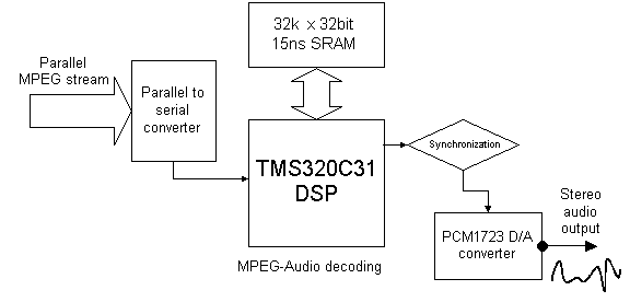
The design of the Whitney hardware is not very complicated. The DSP needs memory and a clock oscillator for its operation, and it has synchronous serial input and output ports. To facilitate the interfacing of Whitney to a host controller (a normal PC or the Axis Printerserver used in the thesis) a Centronics-compatible parallel port was needed though, so logic to perform Centronics handshaking and parallel-serial conversion was needed. Also the serial output from the DSP differs slightly from the kind of input expected by the D/A-converter so some gluelogic was necessary there as well.
From the outside, the TMS320C31 DSP looks much like any other CPU. It has a 24-bit adress bus, a 32-bit data bus, interrupt signals and a lot of miscellaneous control signals. The DSP runs at 60 MHz, but has an internal instruction and data-fetching cycle of half that speed, that is, 30 MHz. To reach maximum speed, it was imperative that the external RAM should be zero-waitstate, in other words, the access-time including circuit-board and adress decoding delays had to be under 33 ns. The memory could be mapped directly based on physical adress 0 in the DSP though, so no adress decoding had to be done. Axis already had an in-stock SRAM memory unit of 32 k x 8 bits at 15 ns access, so it was a simple matter of connecting four of those in parallel directly to the adress- and databus of the DSP and the access time would be fast enough.
The DSP has a high-speed synchronous serial port with simultaneous input and output capabilities. When the DSP is reset, it starts reading words from the serial input, and loads them into memory, then executes that code. The input port should then be used for accepting MPEG-audio streamed data coming from the parallel interface. It was easiest to combine the boot-loading and MPEG streaming so that the unit also boots from data from the parallel port. Logic that would accept 8-bit words from the parallel port, handshake with the port, and serializing them into the DSP's serial input port, was necessary. The maximum serial clocking speed of the DSP is 11.5 MHz, so the 30 MHz clock was divided by four to provide a clocking speed of 7.5 MHz. The unit also had to generate a frame synchronization pulse to the DSP at the start of every fourth byte, since the DSP only accepts 32-bit words at the serial input when boot-loading. It would be a rather complex state-machine so a MACH-210 reprogrammable logic device from AMD with 64 flip-flops was used.
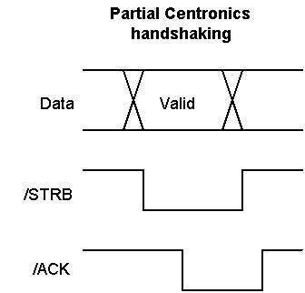
The Centronics standard is a standard for handshaking 8-bit parallel data, and consists of an interface with eight datalines, a strobe signal (STRB), an acknowledge signal (ACK) and some more flow-control (BUSY) and error reporting (ERROR, PAPEROUT) signals. The procedure to send a byte of data is as follows: data is put on the eight data lines by the sending device (the host) and the STRB signal goes active to signal that data is available. The receiving device (the slave) latches the data, and responds by setting the ACK signal. The host detects this and releases the STRB, whereupon the slave releases the ACK, and the transfer is completed. The handshaking with the STRB and ACK signals is illustrated in the picture below. The MPEG decoding software in the DSP can control the BUSY signal to stop the host's sending of data when the internal buffer is full.
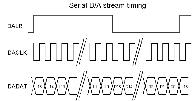
The serial output from the DSP, should be connected more or less directly into the D/A-converter since it has a serial input port. Unfortunately there was a slight complication - the D/A accepts 16-bit words from each channel in an interleaved fashion, and needs a signal that is active or in-active depending on if it is the left or right channel word on the line. The DSP cannot produce such a signal when transmitting 32-bit words - it can only generate a frame-synchronization pulse at the beginning of each 32-bit transfer. Therefore another state-machine had to be implemented in the MACH which waits for the synchronization from the DSP, sets the Left/Right signal to Left, counts 16 transmitted bits, then sets the signal to Right, and waits for 16 more bits. The DSP generates its serial clock itself, by internally dividing the provided 27 MHz clock according to the chosen samplerate (44.1 kHz in Whitney). The timing diagram for the Left/Right signal is shown below:
The final logic-code written in MACHXL format is available in Appendix B.
The rest of the digital circuitry consists of buffer-circuits for the parallel port, and two clock-generators for the DSP and the D/A. The analog circuitry contains a switching power-supply capable of being fed with both AC and DC at a quite broad range of voltages, easily meeting the 9-12 volt requirement. It also contains a stereo 12 watts integrated power amplifier, a TDA1518BQ that can drive two loudspeakers if necessary, and a small reset-circuit that generates a reset-pulse whenever the power is cycled. Filters in the form of a capacitor and a coil are placed at the D/A-converters voltage feeds to reduce the overhearing of noise from the power-rails.
A picture of the PCB CAM layout including component placements, can be found in Appendix C.
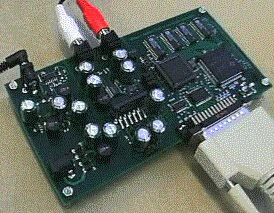
The switching power-supply is in the upper left-hand corner, at the power-connector. To the right of it, just below the phono connectors (with the white and red cables in the picture), is the D/A-converter and associated power supply filters. In the lower left section, is the stereo power amplifier along with its separate power input in the lower left corner of the board. The entire right section of the board contains the digital system of chips, including the DSP in the lower right corner, the four SRAM chips in the upper right corner, the socketed MACH210 programmable logic chip in the middle and some buffer chips just above the parallel port.
The common PCB process used by Axis for thesis projects, allows for four-layer boards. The normal layer allocation used for such boards is to use the top and bottom layers for signal routing, and the two middle-layers for power and ground planes, to ensure good noise and spike tolerance while providing a good current supply for all components regardless location, so that is what was used for Whitney as well.
The PCB layout program used was PowerPCB with manual routing. That means that the designed schematics were imported from PADS-Logic and all PCB circuit tracks were drawn manually. This resulted in a very compact digital part of the circuit board (the right part, in the picture), with almost all tracks on the upper side of the board.
Previous chapter: Implementation of MPEG-Audio, next chapter: Network interface
This document may be freely distributed for educational purposes. See the copyright notice for additional information.