| |
All
material pertains to both Virtex and Virtex-E unless specifically noted in parentheses.
The Xilinx Virtex-E Family: Bandwidth Solution for Next Generation High Performance SystemsWith the introduction of the Virtex series, Xilinx redefined the field programmable gate array (FPGA). Unparalleled density and performance coupled with a powerful set of system level features enables designers to architect their systems with the Virtex capabilities at the core.As a result of being designed in system critical applications, the measuring criteria of an FPGA has grown from the traditional measurements of density and performance to include bandwidth capability. Bandwidth is the measure of how many actions can be accomplished in a given amount of time and is the key differentiating factor for many end products. Computing architectures measured in million instructions per second (MIPS) and data communication systems measured in gigabits per second highlight the importance of bandwidth. The new Virtex-E family of FPGAs is built on the highly successful Virtex architecture.
Leveraging the 0.18-micron, six-layer metal technology, Virtex-E devices push
the traditional FPGA measurements to two million gates, 804 I/Os and over 311
Megabits per second (Mbps) performance. Combined with system level features for
clock management, multiple standard I/O, and embedded True Dual-Port memory, the
Virtex-E family is designed to support the bandwidth requirements of next generation
high performance systems.
I/O Bandwidth Scalable to 200 Gigabits per second (Gbps) The I/O bandwidth is calculated by multiplying 311 Mbps I/O performance rate times 80 percent of the maximum usable I/O numberwhere 80 percent is the assumption used for a typical percentage of the device's I/Os used as data signals. It is very likely that a given design will require multiple high bandwidth data ports with the bandwidth distributed across the required ports. For next generation systems, port bandwidth on the order of 10 Gbps such as OC-192 data rates is the leading edge. With the high bandwidth capability supported by the Virtex-E architecture, several 10 Gbps ports can be achieved within a single device. Bandwidth Enabling Technology Simply having input and output pins that can toggle at high frequencies is only one part of the complete solution for addressing next generation bandwidth requirements. Precise clock management that controls timing relationships between external clock and data must allow the device to interface with a variety of external components with some flexibility. Once the high bandwidth is captured at the device pins, capabilities for internal memory and logic must process the data at the required bandwidth. Furthermore, to communicate with external interfaces (such as with high-speed external memory or system backplanes) the device pins must address a variety of signal standards. The Virtex-E devices contain advanced system technology to support the bandwidth requirements throughout the system. The illustration below shows a block diagram of the Virtex-E bandwidth enabling technology including 100 percent digital delay lock loops (DLL), True Dual-Port embedded memory and SelectI/O+ technology to address these areas of high-bandwidth support.
Virtex-E Architecture Overview 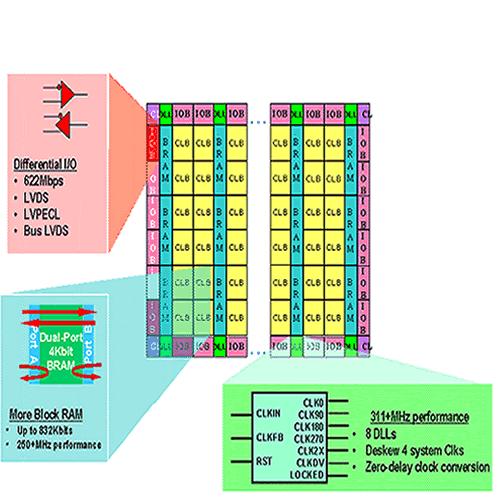
Eight High Performance DLLs - Drop-in Bandwidth Optimization Supporting the highest bandwidth data
rates between devices requires advanced clock management technology such as DLL.
The DLL circuitry allows for very precise synchronization of external and internal
clocks. Xilinx was the first to deliver DLLs in programmable logic by offering
four 200 MHz DLLs in every Virtex device. The Virtex-E family takes this technology
to the next level with devices containing eight DLLs capable of over 311 MHz.
As a fully digital implementation, the Virtex and Virtex-E DLLs do not have the
typical problems of an analog phase locked loop (PLL) including board isolation
and decoupling of power and ground. Virtex-E DLLs provide precise clock edges
through phase shifting, frequency multiplication, and frequency division. The
precise duty cycle generation is critical for high performance applications (like
Double Data Rate, or DDR) in which a slight shift in duty cycle can dramatically
decrease overall system performance.
DLL Application Notes and Reference Designs
Maximizing Double Data Rate Memory Bandwidth with Virtex-E DLL A key technique
for increasing the bandwidth of a particular data port is to have signals change
on both edges of a clock, commonly referred to as the Double Data Rate technique.
Memory suppliers have already started to support this type of high performance
technique to increase the memory bandwidth of their devices. At high frequencies,
signal integrity limits the clock performance, which limits the bandwidth of the
data. Bandwidth for the port is immediately doubled if the architecture can change
data at each edge of a system clock. It is critical that a clock duty cycle is
very precise to 50 percent for this technique. Since Virtex-E DLLs can generate
clocks with a duty cycle guaranteed to be within 100 picoseconds (Ps) of 50 percent;
system designers can achieve the maximum memory bandwidth in the DDR application.
The following diagram demonstrates how Virtex-E DLLs help achieve maximum bandwidth
in a 266 MHz DDR application. For more details regarding DLL, please see the DLL
Tech Topic. 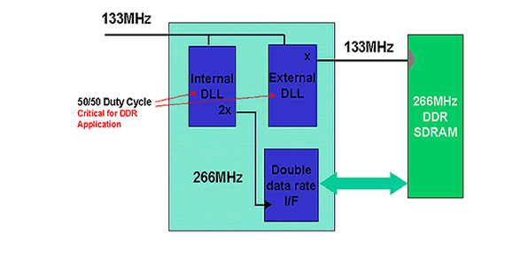
SelectI/O+ Technology: Flexibility, High Bandwidth, and Superior Signal Integrity In order to meet the
bandwidth requirements, electrical signals need to travel on a printed circuit
board over 100 MHz, standard TTL and CMOS signal technology cannot keep pace.
With the Virtex series, Xilinx pioneered the SelectI/O technology designed to
support 200 MHz I/O and allow a single device to interface to any device without
external converters. Virtex-E SelectI/O+ technology expands the performance and
flexibility by supporting high performance I/O standards such as HSTL and SSTL
at over 311 Mbps per pin. In addition, Virtex-E devices are the first programmable
logic device to directly interface to differential I/O standards including LVDS,
Bus LVDS (BLVDS) and LVPECL. The Virtex-E family offers a hierarchy of differential
support, including up to 36 I/O pairs for LVDS and LVPECL operating at 622 Mbps,
and up to 344 differential pairs operating at over 311 Mbps. Support for up to
344 differential pairs capable of over 311 Mbps provides maximum bandwidth of
over 100 Gbps, which can be distributed over the three differential signal standards
as needed. For the first time in a programmable device, system designers can leverage
the high bandwidth and noise immunity characteristics of these standards. For
more information, see Table
of Standards Supported Virtex-E Aggregate Bandwidth Summary
High-Performance Differential Signaling: LVPECL, LVDS, and Bus LVDS Typical aggregate bandwidth requirements for leading edge systems are exceeding 100 Gbps. Increasingly, leading systems designers are turning to differential signaling as the mechanism of choice for these requirements. Differential signaling enables high bandwidth while reducing power, increasing noise immunity, and decreasing EMI emissions. Virtex-E devices meet this emerging challenge with unprecedented capabilities and support for high-performance differential signaling. Virtex-E SelectI/O+ technology addresses the three leading industry-standard differential signaling standards: LVPECL, LVDS, and Bus LVDS (BLVDS). LVPECL I/O is widely used in 100+ MHz inter-chip signaling in high-speed data communications and instrumentation systems. Fiber-Optic Network Interfaces and gigahertz Analog-to-Digital Converters, for example, rely on LVPECL I/O to achieve gigabit per second bandwidth. All Virtex-E I/Os support LVPECL input, output, and I/O signaling. This unparalleled flexibility enables users to create interfaces to hundreds of industry-standard LVPECL devices. In addition to high-speed interfacing, LVPECL is the industry standard for transmission of precise, onboard clocks at frequencies in excess of 100 MHz. While traditional LVTTL clock sources are typically limited to 100 MHz and below (due to the fundamental signal integrity limits), LVPECL clock sources provide operation up to 400 MHz. As FPGA system clock frequencies exceed 100 MHz, LVPECL clocking becomes an essential requirement. The Virtex-E device supports high-performance LVPECL clock inputs for global and local clocking, with frequencies in excess of 300 MHz. In addition, through the use of its multiple DLLs coupled with SelectI/O+ technology, the Virtex-E devices enable zero-delay conversion of precise LVPECL clocks into virtually any required I/O standard. This facilitates the use of Virtex-E FPGAs as an integral part of high-performance board-level clock distribution strategies. In addition to LVPECL, the
Virtex-E family has the industrys first programmable devices to support Low-Voltage
Differential Signaling (LVDS). LVDS exists in two commonly available variants,
LVDS and Bus LVDS. LVDS is optimized for high-speed point-to-point links, while
Bus LVDS is optimized for backplane applications employing Multi-Drop (One Transmitter,
Multiple Receiver), and MultiPoint (Multiple Transmitters and Receivers) configurations.
The Virtex-E device provides unparalleled support for both LVDS and Bus LVDS,
with support on all devices and speed grades, and up to 688 pins (344 pairs) of
LVDS and/or Bus LVDS capabilities on the largest device, providing an aggregate
bandwidth in excess of 100 Gbps. The Virtex-E Bus LVDS I/Os are fully compatible
with industry-standard Bus LVDS devices from National Semiconductor and other
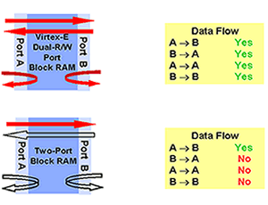
vendors. True Dual-Port Embedded Block Memory for Highest Internal Memory Bandwidth Whether
used as FIFOs to buffer data on and off chip, caches for high speed parallel searches,
or ATM packet buffers, the system requirements for more memory grows much faster
than it does for the requirement for more logic. Xilinx pioneered using embedded
distributed memory (with its SelectRAM+ technology) in its XC4000 FPGAs to allow
the configurable logic block to support logic or memory. With the Virtex series,
this technology was enhanced to include up to 128 Kbits of True Dual-Port fast-embedded
block RAM. The Virtex-E family again provides a quantum leap in internal memory
bandwidth by supporting up to 832 Kbits of True Dual-Port RAM (208 blocks of 4Kbits
memory) capable of 250 MHz performance.
Each True Dual-Port memory block supports 4 Kbits of memory. Each port can
be configured separately to support a variety of depth/width combinations. Embedded
memory can serve to buffer high bandwidth data as well as reduce the internal
processing speed by transparently converting from one data width to another. The
diagram below demonstrates an OC-192 application example. A data port with OC-192
bandwidth comes in on 32 BLVDS pairs running at 311 Mbps per pair. Eight blocks
of embedded RAM are used to buffer the data internally. The port taking data from
the I/O register to the memory is configured as one Kbit deep by 32. The port
leading to the internal processing of the data is configured as 256 by 128. Internal
processing of the 128-bit data need only run at 78 MHz to keep up with the OC-192
bandwidth. An outgoing port would be configured similarly. 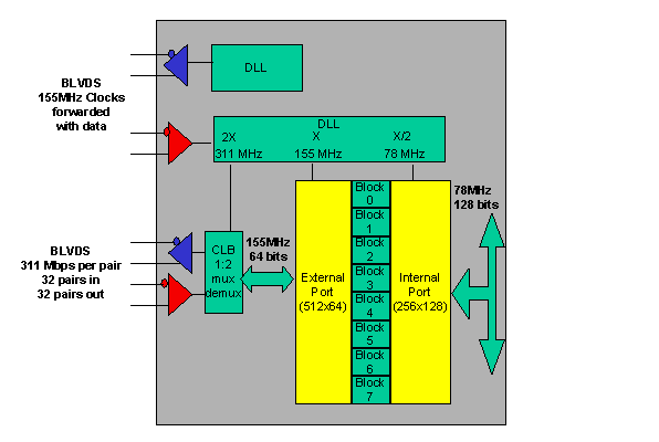
Completing the Solution with Packaging, Software and Intellectual Property To support tens of gigabits per second bandwidth through a device, the package must be capable of packing many high performance I/Os in limited board space. At the same time, package power characteristics may be required to dissipate several watts of power for the highest bandwidth applications. Virtex-E devices continue the tradition of the industry's most reliable and flexible packaging. Mainstream plastic quad flat pack (PQFP) and 1.27 mm ball grid array (BGA) as well as leading edge 0.8 mm chip scale package (CSP) and 1.0 mm fine pitch BGA (FG) are supported across the family. For the fine pitch 1.0 mm BGA offering, the Virtex-E family introduces three new FG packages: 31 mm by 31 mm FG900; 35 mm by 35 mm FG1156; and a thermally enhanced 42.5 mm by 42.5 mm FG860. The Virtex-E family can now support up to 804 I/Os with a board real estate as small as 35 mm by 35 mm. These packages set new standards in I/Os per square inch as well as maximum bandwidth per square inch. Squeezing all the bandwidth capabilities of the three million gate XCV3200E device will likely be distributed among multiple digital designers. Xilinx introduced Virtex-E support with version 2.1i software that further reduced the industry leading compile times by an additional 50 percent as well as delivered the Xilinx Internet Team Design tools to coordinate communication between designers resulting in optimized design cycles. Smart-IP technology allows Xilinx to offer architecture independent IP that provides the best in predictability, flexibility and performance. The CORE Generator 2.1i tools support the Virtex-E devices at silicon availability. Popular high bandwidth cores including the Real-PCI 64/66 solution and the 32/33 Xilinx LogiCORE PCI solution support Virtex-E devices today. With the capabilities of the Virtex-E architecture coupled with Xilinx LogiCORE, AllianceCORE and XPERTs programs, many high bandwidth cores are in development. For up to date information on the latest cores, contact Xilinx IP Center at www.xilinx.com/ipcenter. Summary Demonstrated by unprecedented adoption rate, Virtex series redefined the FPGA
with a feature set that moved FPGAs from glue logic to the core of the system
design. With the significant performance and flexibility enhancements in the areas
of clock management, SelectI/O+ technology, True Dual-Port block memory, and high
performance differential signaling support, the Virtex-E family is well set to
continue the success of Virtex platform by enabling system designers to meet the
bandwidth requirement of the next generation high performance systems. By supporting
overall bandwidth requirements previously addressed only by inflexible ASIC technology,
Virtex-E devices will further increase the application space for programmable
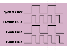
logic. System Timing Solution (Virtex)HighlightsThe Virtex family solves clock skew issues by allowing internal and external clock synchronization. With four Delay Locked Loops, your system's clock skew will be removed. You can get clock-to-output delays of less than three nanoseconds and very substantial increases in system performance.
As FPGAs grow in size, quality on-chip clock distribution becomes increasingly important. Clock skew and clock delay impact device performance and the task of managing clock skew and clock delay with conventional clock trees becomes more difficult in large devices. The Virtex series of devices resolve this potential problem by providing four fully digital dedicated on-chip Delay-Locked Loop (DLL) circuits which provide zero propagation delay and zero clock skew between output clock signals distributed throughout the device. Each DLL can drive up to two global clock routing networks within the device. The global clock distribution network minimizes clock skews due to loading differences. By monitoring a sample of the DLL output clock, the DLL can compensate for the delay on the routing network, effectively eliminating the delay from the external input port to the individual clock loads within the device. In addition to providing zero clock skew and zero delay with respect to a user source clock, the DLL can provide multiple phases of the source clock. The DLL can also act as a clock doubler or it can divide the user source clock by up to 16. Clock multiplication gives you a number of design alternatives. For instance, a 50 MHz source clock doubled by the DLL can drive an FPGA design operating at 100 MHz. This technique can simplify board design because the clock path on the board no longer distributes such a high-speed signal. A multiplied clock also provides designers the option of time-domain-multiplexing, using one circuit twice per clock cycle, consuming less area than two copies of the same circuit. To increase the effective clock multiplication factor to four, you can connect two DLLs in series. The DLL can also act as a clock mirror. By driving the DLL output off-chip and then back in again, you can use the DLL to deskew a board level clock between multiple devices. In order to guarantee the system clock establishes prior to the device waking up, the DLL can delay the completion of the device configuration process until after the DLL achieves lock. By taking advantage of the DLL to remove on-chip clock delay, you can greatly simplify and improve system level design involving high-fanout, high-performance clocks. Customer Comments:"Virtex FPGAs have allowed us to implement our next generation digital TV broadcast systems in record time," said John Simmons, project manager, of NDS, a world leader in digital broadcasting solutions. "A key time saver was the availability of multiple DLLs that allowed us to synchronize a 74 MHz clock to more than 30 devices including multiple FPGAs, SDRAMs, and other components. Designing a no-skew clock system from scratch would take months. Xilinx delivered a ready-made solution to us with Virtex FPGAs."We did an exhaustive search and
found that only the Xilinx Virtex FPGAs could provide us with the performance
and density necessary to add Gigabit capability to the Nebula switch family,
said John Peters, vice president of development at Performance Technologies.
We are very impressed with the system level capabilities of the Virtex FPGAs,
particularly the digital delay locked loops and support for multiple I/O standards.
| |||||||||||||||||||||||||||||||||||||||||||||||||||||||||||||||||||||||||||||||||||||||||||||||||||||||||||||||||||||||||||||||||||||||||||||||||||||||||||||