| |
All material pertains to both Virtex and Virtex-E families
unless specifically noted.
System Memory Technical BriefThe newest system designs are requiring higher bandwidth and performance. Synchronous DRAMs (SDRAMs) and Zero Bus Turnaround (ZBT) SRAM (Pipelined and Flowthrough) are frequently used to satisfy the expanded memory requirements. Since time to market is so critical for our customers to reduce the overall system cost and maximize the product revenue, Xilinx is providing all the necessary tools to help you meet your time to market goals.Beyond the obvious benefits of speed and size, the Virtex FPGAs offer enhanced memory-related advantages for both on chip as well as external. The SelectRAM+ memory hierarchy includes:
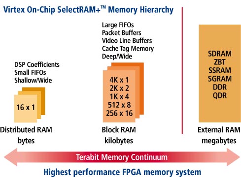
Virtex FPGAs provide access to a variety of on-chip and off-chip RAM resources. In addition to the on-chip Distributed SelectRAM and Block SelectRAM, a Virtex design can also interface directly to megabytes of external high-speed SRAMs and DRAMs. The combination of high speed SelectI/O and on-chip Clock Delay-Locked Loop (DLL) allows systems to operate at maximum RAM speeds. A Virtex interface to a ZBT (Zero Bus Turnaround*) SRAM provides interleaved Read/Write messages without wasteful turnaround cycles. Distributed SelectRAMVirtex FPGAs provide distributed SelectRAM or Look-Up tables configured as small bits of RAM. The distributed SelectRAM can be configured as a single-port 32x1 RAM or a dual-port 16x1 RAM (one read and one write port), or a single-port 16x2 RAM. It provides shallow RAM distributed throughout the chip and is well suited for DSP applications.Block SelectRAMThe next rung of the memory hierarchy is the Block SelectRAM. Available in 4K blocks, each block is a fully-synchronous true dual-port memory. Each port allows reads and writes on independent clocks. Each port can access the memory in 4K x 1, 2K x 2, 1K x4, 512 x 8, or 256 x 16 configurations. As independently-configurable ports, the RAM blocks are used as buffers for high-speed data streams and for funneling data to different width/speed combinations. The blocks can be combined to create wider or deeper memory. The True Dual-Port Block SelectRAM is capable of creating FIFOs with independent clocks running at 250 MHz (170 MHz for the Virtex family). Block SelectRAM offers advantages in many networking and telecommunication applications that require memory updates without delaying read access.High-Speed Memory InterfacesThe third part of the Virtex memory
hierarchy comprises pre-engineered interfaces to off-the-shelf memory parts from
leading memory vendors. The combination of high speed SelectI/O and on-chip CLKDLL
enable the interface to operate at maximum RAM speeds. Off-chip memory solutions
for Virtex design currently include interfaces to ZBT (Zero Bus Turnaround) SRAM
(Pipelined and Flowthrough), SDRAM, and SGRAM reference designs. The pre-engineered
solutions incorporate a synthesizable Verilog net list, timing constraints in
the Xilinx UCF format, and special switches for software where applicable.
Memory Vendors SupportedVirtex and Virtex-E FPGAs support some of the most advanced memories on the market today. Through close relationships with memory vendors, we are able to ensure support for their memory devices through future generations. The table below illustrates some of the vendors supported:
Virtex SDRAM Controller DesignSDRAMs provide significant improvement in bandwidth performance over traditional asynchronous DRAMs such as "FPM" (Fast Page Mode) and "EDO" (Extended Data Out) devices. SDRAMs latch input address, data, and control signals on the clock rising edge, thus freeing the controller from having to drive address and control for the whole read or write transaction. SDRAMs offer features to enhance overall bandwidth performance, such as multiple internal banks, burst mode access, and pipelining of operation executions. SDRAMs are becoming available in speed grades above 100 MHz using LVTTL IOs. The Virtex FPGAs have many features, such as the SelectI/O and the Clock Delay Lock Loop(DLL), that make it easy to interface to high speed SDRAMs. The block diagram in Figure 1 shows how a Virtex FPGA interface to the SDRAMs. The Virtex Synthesizable High Performance SDRAM controller application note describes the design and implementation of a synthesizable, parameterizable, flexible, auto-placed-and-routed SDRAM controller with the Virtex FPGA device. A 32-bit wide data interface version can run up to 125 MHz when automatically placed and routed in a Virtex -6 speed grade device. Hand placed versions of the design will run even faster.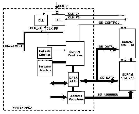 SDRAM controllers vary significantly in features, complexity, and performance. Xilinx provides an application note describing common issues faced by designers designing an SDRAM controller. The reference design, written in Verilog HDL language, is easily modified to fit different memory organization or processor speed and bandwidth requirements. Some programmable interface features that are supported in the SDRAM controller are described in the application note. They can be implemented without requiring a change in the Verilog code. Other less popular features are not programmable and will require a code change. Design trade-off and features for the current SDRAM controller are listed below.
SDRAM Controller Application Notes and Reference Designs
Virtex ZBT SRAM Controller DesignFigure 2 shows a simple interface between a Virtex device and a ZBT SRAM. In addition to the mandatory Address and Data signals, the interface only needs a Read/Write (RW) control signal. To ensure high performance, the design uses two CLKDLLs, one to de-skew and generate a 2X controller clock and another to de-skew and generate a board-level 2X clock. The result is a high-speed de-skewed clock driving the controller and the ZBT SRAM.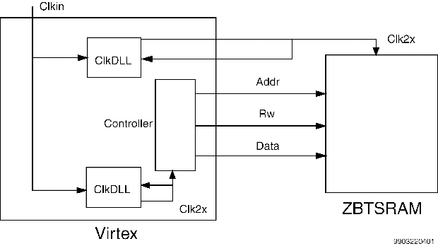
The ZBT SRAMs
are available with LVTTL I/Os. The Virtex SelectI/O supports LVTTL signaling with
a range of driver strengths from 2 mA to 24 mA and a choice of fast or slow slew
rates. A ZBT SRAM controller design in synthesizable Verilog for a 64K x
36 pipelined device as well as for a 64K x 36 flowthrough device is provided
in the design code. Controllers for other size ZBT SRAMs are easily derived from
these designs. In these examples, Read/Write is the only control signal. It is
used to control the Tri-state drivers for the 36 bits of data. In order
to run the Virtex Pipelined ZBT SRAM interface at 200 MHz (100 MHz for flow through)
it uses CLKDLLs to de-skew and double clock frequency. During a write operation
to the pipelined ZBT SRAM, data must be provided to the RAM two cycles after the
Address and Control signals. Assuming that data arrives in lock step with Address
and Control, the controller drives the data to the RAM through two pipelined stages.
While the control signals to the RAM are sent directly, the control signals inside
the controller are delayed through an equal number of pipelined stages to match
the data latency. The pipelined example uses a Flip-flop tree to minimize the
fan-out for the Read/Write signal, which in turn facilitates high-speed data access.
Virtex SelectI/O provides a wide variety of standards and for LVTTL, it offers
a wide range of driver strengths. For more detail of this design, please see the
Virtex ZBT SRAM controller reference design page.
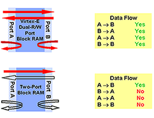
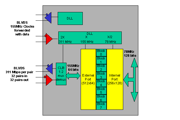
True Dual-Port Embedded Block Memory for Highest Internal Memory BandwidthWhether used as FIFOs to buffer data on and off chip, caches for high speed parallel searches, or ATM packet buffers, the system requirements for more memory grows much faster than it does for the requirement for more logic. Xilinx pioneered using embedded distributed memory (with its SelectRAM technology) in its XC4000 FPGAs to allow the configurable logic block to support logic or memory. With the Virtex series, this technology was enhanced to include up to 128 Kbits of True Dual-Port fast-embedded block RAM. The Virtex-E family again provides a quantum leap in internal memory bandwidth by supporting up to 832Kbits of True Dual-Port RAM (208 blocks of 4Kbits memory) capable of 250 MHz performance.
Each True Dual-Port memory block supports 4 Kbits of memory. Each port can
be configured separately to support a variety of depth/width combinations. Embedded
memory can serve to buffer high bandwidth data as well as reduce the internal
processing speed by transparently converting from one data width to another. The
diagram below demonstrates an OC-192 application example. A data port with OC-192
bandwidth comes in on 32 BLVDS pairs running at 311 Mbits per second per pair.
Eight blocks of embedded RAM are used to buffer the data internally. The port
taking data from the I/O register to the memory is configured as one Kbit deep
by 32. The port leading to the internal processing of the data is configured as
256 by 128. Internal processing of the 128-bit data need only run at 78 MHz to
keep up with the OC-192 bandwidth. An outgoing port would be configured similarly.
CAM (Content Addressable Memory)A Content Addressable Memory is a storage array designed to quickly find the location of a particular stored value. By comparing the input against the data memory, a CAM determines if an input value matches one or more values stored in the array. If the comparison is done simultaneously, the CAM is said to be at maximum efficiency. A match, when it exists, is found in one clock cycle. Similar to a RAM, a CAM stores words in an array. The write mode is comparable, but the read mode is different. In a RAM, the word in a specific location is read by the address. In a CAM, the data on the input is looking for a match. When a match is found, the output is the address in the array. The number of address lines limits a RAMs data size. For example, a 10-bit bus addresses 1024 locations of 8-bit data. A CAM does not have this limitation because it does not use an address bus to read a location. To find a match of an 8-bit value in 1024 locations, an 8-bit bus on the input is required. When the data is found in the CAM, a match signal goes active. The output is the matching data address. Because a CAM does not need address lines to find data (read mode), the memory size can be easily extended. The width is determined by the storage and com-parator size. The basic core of a CAM has a storage location, and a comparator between the storage location value and the input data. This application note describes the different ways to design a basic core optimized for either speed, density, or both. CAMs are used in telecommunications, networking, Ethernet, ATM switches and diverse protocol applications. To determine the correct CAM implementation for a particular application, the following should be investigated.
Virtex devices offer the advantage of different approaches to designing an optimal CAM. There is not a specific CAM type to fit all typical CAM applications and different approaches produce an optimal results. CAM Application Notes and Reference Designs
Double Data Rate SDRAMAs microprocessors get faster every year, memory architectures are also changing in order to improve the overall system performance. DDR SDRAM and RDRAM (Direct RAMBUS DRAM) are the top two contenders for the next generation of SDRAM. While RDRAM is a revolutionary change, DDR SDRAM is a natural evolution from the existing SDRAM architecture. RDRAM has a peak bandwidth of 1.6 Gbytes/s with 16-bit lines and a 400 MHz clock frequency. DDR SDRAM also has a peak bandwidth of 1.6 Gbytes/s with 64-bit data lines and a 100 MHz clock frequency. The main advantage of DDR SDRAMs over RDRAMs is the use of the basic system infrastructure developed for PC-100. This eliminates the numerous design changes required by different "packet" protocols. DDR SDRAM was approved as a JEDEC (Joint Electron Device Engineering Council) standard in February, 1998, and is currently supported by most major SDRAM vendors.
Customer Comments"Using a Virtex XCV300 FPGA, I was able to meet the design requirement of a 100 MHz,512K by 32 pipelined ZBT SRAM interface, which is part of our patented Gigabyte Compression(TM) technology," said Winefred Washington, senior hardware engineer at Interactive Silicon, an Austin, Texas, company that licenses intellectual property to semiconductor manufacturers. "The clock frequency
of the SDRAM interface is our major bottleneck in providing higher "The Virtex parts were also the most advanced that we could find", says Jim Crysdale, Sr. Staff Engineer & Manager at Qualcomm. "The block memory was very important because we need a lot of storage to store data. Obviously when youre running data networks you have to store data, and the fact that we had on-chip RAM was very enabling to us." "Because it is a high density, high capacity device, the Xilinx FPGA allows us to provide very large capacity emulators to meet our customers' needs," said Juergen Jaeger, Director of Emulation Product Management for IKOS. IKOS has traditionally used external memory devices such as SRAM, but are now beginning to take advantage of the internal memory. "The obvious result of using the embedded RAM of the FPGA is an increase in the speed and efficiency of our products. The device allows us to build upon our already successful architecture," said Jaeger. The availability of large amounts of block SelectRAM in
the Vid chip also allowed us to implement many of our sophisticated post-processing
algorithms, said John Snow, PC Simulation Engineering Manager at Evans
& Sutherland.
| |||||||||||||||||||||||||||||||||||||||||||||||||||||