| |
| Fusion Devices |
AFS090 |
AFS250 |
AFS600 |
AFS1500 |
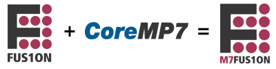
| ARM-Enabled Fusion Devices |
|
|
M7AFS600 |
M7AFS1500 |
 |
System Gates |
90,000 |
250,000 |
600,000 |
1,500,000 |
| Tiles (D-Flip-Flops) |
2,304 |
6,144 |
13,824 |
38,400 |
| Usable Tiles with CoreMP7S 1 |
|
|
7,500 |
32,000 |
| Usable Tiles with CoreMP7Sd 1 |
|
|
5,237 |
29,878 |
| Secure (AES) ISP |
Yes |
Yes |
Yes |
Yes |
| PLLs |
1 |
1 |
2 |
2 |
| Globals |
18 |
18 |
18 |
18 |
 |
Flash Memory Blocks
(2 Mbits) |
1 |
1 |
2 |
4 |
Total Flash Memory Bits
(Mbits) |
2 |
2 |
4 |
8 |
FlashROM Bits
(kbits) |
1 |
1 |
1 |
1 |
RAM Blocks 1
(4,608 bits) |
6 |
8 |
24 |
60 |
RAM
(kbits) |
27 |
36 |
108 |
270 |
 |
Analog Quads |
5 |
6 |
10 |
10 |
| Analog Input Channels |
15 |
18 |
30 |
30 |
| Gate Driver Outputs |
5 |
6 |
10 |
10 |
| I/O Banks (+ JTAG) |
4 |
4 |
5 |
5 |
| Maximum Digital I/Os 2 |
75 |
114 |
172 |
278 |
| Analog I/Os |
20 |
24 |
40 |
40 |
 |
QN108 |
37/9 (16) |
|
|
|
| QN180 |
60/16 (20) |
65/15 (24) |
|
|
| PQ208 |
|
93/26 (24) |
95/46 (40) |
|
| FG256 |
75/22 (20) |
114/37 (24) |
119/58 (40) |
119/58 (40) |
| FG484 |
|
|
172/86 (40) |
228/86 (40) |
| FG676 |
|
|
|
278/139 (40) |
Notes:
1 Refer to the CoreMP7 datasheet for more information.
2 Some debug tools require 10 digital I/Os for external connection.

 |
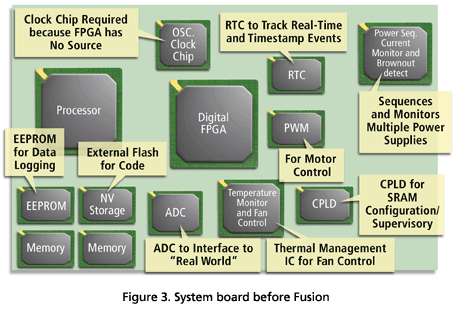
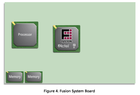
Single Chip
Flash-based FPGAs store the configuration information in on-chip Flash cells. Once programmed, the configuration data
is an inherent part of the FPGA structure and no external configuration data load is required at system power-up. Flash-based
Fusion FPGAs do not require additional system components such as configuration serial nonvolatile memory
(EEPROM) or a Flash-based microcontroller in order to load the device configuration data at every system power-up.
Increased Fusion functionality can remove several additional components from the board, such as Flash memory, discrete
analog ICs, clock sources, EEPROM, and real-time clocks, thereby reducing system cost and board space requirements.
|
 |
Low Power
The Actel Flash-based Fusion devices exhibit power characteristics similar to an ASIC, making them an ideal choice for
battery-operated and other power-sensitive applications. With Fusion devices, there is no power-on current surge and
no high-current transition; these do occur on many SRAM FPGAs. Fusion devices also have low static and dynamic power
consumption, further maximizing power savings. These devices support sleep and standby modes of operation to
greatly reduce power consumption. Another unique feature of Fusion is the ability to dynamically shift between normal
clock speeds and low clock operation during periods of inactivity, and switch back to full speed when needed.
|
 |
Live At Power-Up
Flash-based Fusion devices are live at power-up (LAPU). As soon as system power is applied and within normal operating
specifications, Fusion devices are working. The live at power-up feature of Fusion devices greatly simplifies total system
design and often allows for the removal of complex programmable logic devices (CPLDs) from the system. Glitches and
brownouts in system power will not corrupt the Fusion device�s Flash configuration, and unlike SRAM-based FPGAs, the
device will not have to be reloaded when system power is restored. This allows designers to reduce or completely remove
the expensive power sequencing, voltage monitor, and brownout detection devices from PCB. Simplifying the total
system design by using Flash-based Fusion devices reduces cost and design risk while increasing system reliability and
improving system initialization time.
|
 |
Security
Fusion devices incorporate the Actel FlashLock® feature, providing a unique combination of reprogrammability and design
security without external overhead. These advantages can only be offered by an FPGA with nonvolatile Flash memory.
Fusion devices have a 128-bit Flash-based lock and industry-leading on-chip AES decryption core, used to secure
programmed IP and configuration data. The AES-128-block cipher is a faster, more secure government-approved
replacement for DES. Fusion devices have the most comprehensive programmable logic device security solution available
today. Fusion devices with AES-based security allow for secure, remote field updates of both system design and Flash
memory content (over public networks such as the Internet), and ensure that valuable intellectual property remains out
of the hands of system overbuilders, system cloners, and IP thieves. The FPGA design of programmed Fusion devices
cannot be read back, though secure (AES-based) design verification is possible. Many device design and layout
techniques have been used to make invasive attacks extremely difficult. For example, Flash cells are located beneath
seven metal layers, making tampering with the Flash elements extremely difficult. Care has been taken to remove single
points of attack in the device�s programming control logic.
|
 |
Firm Errors
Firm errors occur when high-energy neutrons, generated in the upper atmosphere, strike a configuration cell of an
SRAM FPGA. The energy of the collision can change the state of the configuration cell in SRAM FPGAs and thus change
the logic, routing, or I/Os in an unpredictable and uncontrollable way. These errors are impossible to prevent in SRAM
FPGAs and can result in failure-in-time (FIT) rates in the thousands. The consequences of these types of errors may result
in a complete system failure and major support and product liability issues. The configuration element of Fusion FPGAs,
the Flash cell, cannot be altered by high-energy neutrons and is therefore immune to neutron effects.
|
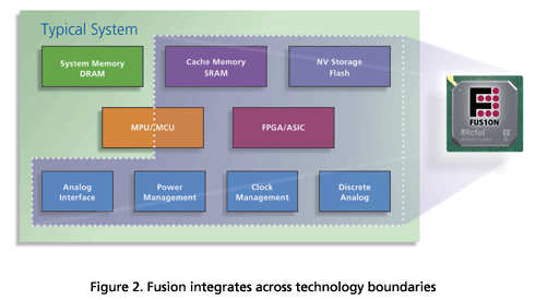
Move the cursor over the numbers below to learn more about Fusion Programmable System Chip architecture.
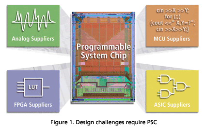
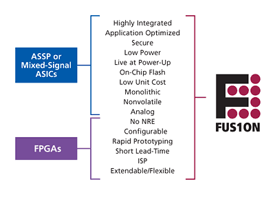
One Chip is All You Need
Until now, system designers were forced to choose costly and space-consuming
discrete analog components with programmable logic or mixed-signal ASIC
solutions to implement a typical system. Fixed architectures and other
technology barriers prevented the integration of individual components into
a single, low cost chip that met all design requirements.
Real World Interface
 Fusion interfaces to the real world; up to 30 high-voltage-tolerant analog
inputs enable direct connection to signals from �12 V to +12 V, eliminating
the need for signal preconditioning. The Fusion analog to digital converter
(ADC) is configurable and supports resolutions up to 12 bits, and sample
rates up to 600 k samples per second (ksps). Fusion adds additional
functionality with the inclusion of multiple differential input current
monitor blocks, each with a built-in amplifier, increasing sensitivity and
efficiency. The Fusion integrated temperature monitor circuitry allows for
the monitoring of multiple remote temperatures with only an external diode
needed. Up to ten high current drive outputs are ideal for metal-oxide
semiconductor field-effect transistor (MOSFET) control and/or pulse
width modulation (PWM) functions such as direct fan control.
Fusion interfaces to the real world; up to 30 high-voltage-tolerant analog
inputs enable direct connection to signals from �12 V to +12 V, eliminating
the need for signal preconditioning. The Fusion analog to digital converter
(ADC) is configurable and supports resolutions up to 12 bits, and sample
rates up to 600 k samples per second (ksps). Fusion adds additional
functionality with the inclusion of multiple differential input current
monitor blocks, each with a built-in amplifier, increasing sensitivity and
efficiency. The Fusion integrated temperature monitor circuitry allows for
the monitoring of multiple remote temperatures with only an external diode
needed. Up to ten high current drive outputs are ideal for metal-oxide
semiconductor field-effect transistor (MOSFET) control and/or pulse
width modulation (PWM) functions such as direct fan control.
Power and Thermal Management
Fusion is Level 0 live at power-up (LAPU) and can be run from a single 3.3
V power supply. These simple startup requirements enable Fusion to act as
the ultimate system manager, capable of monitoring and sequencing
 multiple power supplies to bring up your board in a controlled manner. The
ramp-rate of each power supply is programmable from the Fusion device.
Fusion easily integrates thermal management aspects of system control boards
by combining its temperature monitor and MOSFET/PWM capabilities.
multiple power supplies to bring up your board in a controlled manner. The
ramp-rate of each power supply is programmable from the Fusion device.
Fusion easily integrates thermal management aspects of system control boards
by combining its temperature monitor and MOSFET/PWM capabilities.
Dynamic System Configuration
The ability of Fusion devices to support many system-level functions in a
single chip makes Fusion an ideal candidate for leading edge system
management protocols.
 Fusion high performance Flash memory blocks provide nonvolatile memory
flexibility to every aspect of your design. At system startup, the Flash
memory can be used to initialize the system. SRAMs and registers can be
automatically loaded with data from the on-chip Flash memory. Prior to
system shutdown, the volatile values in SRAM or registers on the Fusion
device can be saved back into the on-chip Flash memory�saving the state
of the device for the next system startup (SAVE and RESTORE). The
Fusion Flash memory also enables the dynamic changing
of system parameters (CONTEXT switch). System
boot codes can be stored in the Flash memory for both
on-chip and off-chip requirements. The Flash memory
can be configured to emulate EEPROM operation with
an available endurance extender IP. The optional use of
the soft IP Common Flash Interface (CFI) core from
Actel enables use of part of the Flash memory for file storage.
Fusion high performance Flash memory blocks provide nonvolatile memory
flexibility to every aspect of your design. At system startup, the Flash
memory can be used to initialize the system. SRAMs and registers can be
automatically loaded with data from the on-chip Flash memory. Prior to
system shutdown, the volatile values in SRAM or registers on the Fusion
device can be saved back into the on-chip Flash memory�saving the state
of the device for the next system startup (SAVE and RESTORE). The
Fusion Flash memory also enables the dynamic changing
of system parameters (CONTEXT switch). System
boot codes can be stored in the Flash memory for both
on-chip and off-chip requirements. The Flash memory
can be configured to emulate EEPROM operation with
an available endurance extender IP. The optional use of
the soft IP Common Flash Interface (CFI) core from
Actel enables use of part of the Flash memory for file storage.
Low Power
 Built on a low power, high performance Flash
process, Fusion provides industry leading low static
and dynamic power. Fusion also offers several sleep
and standby modes of operation to further extend
battery life in portable applications. The Fusion Real-
Time Counter (RTC) offers a wide variety of
functionality: sleep, standby, periodic wake-up, and
low speed/power operation. The addition of both a 1% RC oscillator and two-pin
crystal oscillator circuit eliminates the need for
expensive external clock sources.
Built on a low power, high performance Flash
process, Fusion provides industry leading low static
and dynamic power. Fusion also offers several sleep
and standby modes of operation to further extend
battery life in portable applications. The Fusion Real-
Time Counter (RTC) offers a wide variety of
functionality: sleep, standby, periodic wake-up, and
low speed/power operation. The addition of both a 1% RC oscillator and two-pin
crystal oscillator circuit eliminates the need for
expensive external clock sources.
Reconfiguring Systems
Inherent in the fabric of Fusion are the benefits of
configurability and field reprogrammability from the
successful Actel ProASIC®3 family of Flash FPGA
devices. Fusion can be securely programmed late in the
manufacturing process or after it is in the field. By
enabling a single hardware platform to support
multiple projects and products, Fusion allows
designers to leverage economies of scale in purchasing,
while maintaining the ability to customize products for
different markets. Both the firmware (Flash memory)
and hardware can be updated in a single step.
Fusion enabled FPGAs offer the best of both worlds.
Datasheets:
Fusion:
CoreMP7:
CoreAI:
Packaging Data:
Fusion:
ARM7:
Product Information Brochures (PIB): Fusion:
CoreMP7:
|


 Terms and Conditions of Use