There are two clock conditioning cores (CCCs) in SmartGen:
Static PLL
The ProASIC3E CCC includes the following features.
An option to choose the
source of the input clock as one of the following.
Hard-wired I/O
Internal routed net
Other I/O
The option to bypass the PLL for the primary output.
Configuration selections available for frequency, delay and phase.
Configuring a PLL in SmartGen
After you open a new workspace in SmartGen and select one of the Clock Conditioning / PLL cores, you must configure it. To do so:
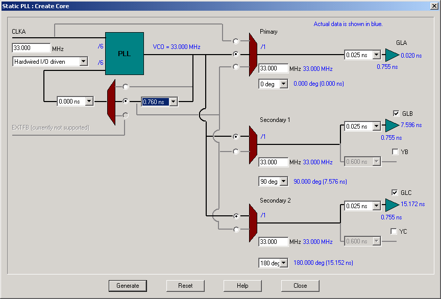
1. Select your output. After you choose to configure the CCC, you must select the number of outputs required. A total of five outputs may be obtained from the CCC. Select the check box next to each required output to select it.
GLA is always selected.
GLB and YB have the same output frequency. They can be delayed by different amounts by setting the individual delays. GLB drives a Global while YB drives a core net. Using only YB also burns the global driver for GLB. However, the global rib is available.
GLC and YC have the same output frequency. They can be delayed by different amounts by setting the individual delays. GLB drives a Global while YB drives a core net. Using only YC also burns the global driver for GLB. However, the global rib is available.
The input signal CLKA is the reference clock for all five outputs.
2. Select your feedback.
Internal Feedback: The source of the feedback signals will be the VCO output signal, with 0 degree phase shift and zero additional time delay (top Selection on the Feedback MUX) or a delayed version of the VCO output, in selectable increments of 600 ps, up to 5.56 ns. This delay advances the feedback clock, thereby advancing all outputs by the delay value specified for the feedback delay element (middle selection of the Feedback MUX).
External Feedback: Not supported in this release.
3. Set your Fixed System Delay. By choosing the non-zero value for this delay, the feedback source signal can be further delayed by a fixed amount of mask delay designed to emulate the delay through the chip’s clock tree. This allows for clock-line de-skewing operations.
4. Specify your input clock.
Input Clock Frequency between 1.5 – 350 MHz
Input Clock Source as one
of the following:
Driven by the hardwired I/O
Driven by an external I/O from a different I/O location
Driven by an internal core net.
5. Specify the primary output. Select source of the output clock.
Output bypassing the PLL (top selection of the GLA MUX). In this case, VCO phase shift and output frequency selection are not available. Output frequency is the same as input frequency in this case.
Output directly from the VCO (middle selection of the GLA MUX). The phase shift of 0, 90, 180, or 270 is available in this case.
Delayed version of the zero phase shift output from the VCO. Phase-shift selection is unavailable for this (bottom selection of the GLA MUX). This output can be used for two purposes: a) to use the feedback delay as an additional delay on the output if feedback advance has not been specified (top and bottom selections of the feedback MUX); b) to compensate for the feedback advance for this particular output if feedback advance has been specified (middle selection of the feedback MUX).
Output frequency (1.5 – 350 MHz)
VCO Phase-Shift (one of 0, 90, 180, or 270 degrees); the phase shift is out of the VCO. The phase shift will be impacted by the value of the divider after the VCO.
An optional Extra Output Delay, in selectable increments of 600 ps, up to 5.56 ns .
6. Specify Secondary1 and Secondary2 Outputs. Select the source of the output clock from the following two choices
Output directly from the VCO (top selection of the GLB/GLC MUX). The phase shift of 0, 90, 180 or 270 is available in this case.
Delayed version of the zero phase shift output from the VCO. Phase-shift selection is unavailable for this (bottom selection of the GLB/GLC MUX). This output can be used for two purposes: a) to use the feedback delay as an additional delay on the output if feedback advance has not been specified (top and bottom selections of the feedback MUX); b) to compensate for the feedback advance for this particular output if feedback advance has been specified (middle selection of the feedback MUX).
Set your Output frequency (1.5 – 350 MHz)
VCO Phase-Shift (one of 0, 90, 180 or 270 degrees); the phase shift is out of the VCO. The phase shift will be impacted by the value of the divider after the VCO.
An individual optional Extra Output Delay for each of the Global and Core outputs, in selectable increments of 600 ps, up to 5.56ns.
When resources are available, the Delay element of the Secondary1 and Secondary2 Global outputs of the CCC can be configured independent of the PLL. The delayed clock is a simple CLKMUX with some additional delay.
Select the programmable delay between 0.280 ns to 5.815 ns, in steps of 160 ps, for the Output.
See Also
Create Clock Conditioning / PLL cores