|

Eight High Performance DLLs - Drop-in
Bandwidth Optimization
Supporting the highest bandwidth data rates between devices
requires advanced clock management technology such as DLL. The DLL
circuitry allows for very precise synchronization of external and
internal clocks. Xilinx was the first to deliver DLLs in
programmable logic by offering four 200 MHz DLLs in every Virtex
device. The Virtex-E family takes this technology to the next level
with devices containing eight DLLs capable of over 311 MHz. As a
fully digital implementation, the Virtex and Virtex-E DLLs do not
have the typical problems of an analog phase locked loop (PLL)
including board isolation and decoupling of power and ground.
Virtex-E DLLs provide precise clock edges through phase shifting,
frequency multiplication, and frequency division. The precise duty
cycle generation is critical for high performance applications (like
Double Data Rate, or DDR) in which a slight shift in duty cycle can
dramatically decrease overall system performance.
Bandwidth Critical Specifications of the Virtex-E DLL
| Parameter |
Value |
| Maximum Output Frequency |
320 MHz* |
| Maximum Output Jitter |
100 ps |
| Output Frequency Duty Cycle |
50%+/- 100 Ps |
* Based on Virtex-E 7 speed grade product
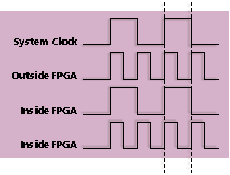
A key technique for increasing the bandwidth of a particular data
port is to have signals change on both edges of a clock, commonly
referred to as the Double Data Rate technique. Memory suppliers have
already started to support this type of high performance technique
to increase the memory bandwidth of their devices. At high
frequencies, signal integrity limits the clock performance, which
limits the bandwidth of the data. Bandwidth for the port is
immediately doubled if the architecture can change data at each edge
of a system clock. It is critical that a clock duty cycle is very
precise to 50 percent for this technique. Since Virtex-E DLLs can
generate clocks with a duty cycle guaranteed to be within 100
picoseconds (Ps) of 50 percent; system designers can achieve the
maximum memory bandwidth in the DDR application. The following
diagram demonstrates how Virtex-E DLLs help achieve maximum
bandwidth in a 266 MHz DDR application.
For more details regarding DLL, please see the DLL
Tech Topic.
System Timing Solution (Virtex)
Highlights
The Virtex family solves clock skew issues by allowing internal
and external clock synchronization. With four Delay Locked Loops,
your system's clock skew will be removed. You can get
clock-to-output delays of less than three nanoseconds and very
substantial increases in system performance.
Fully Digital Delay Locked Loops (DLL)
- Four independent DLL circuits for internal and external
clock synchronization
- 200+ MHz chip-to-chip communication
- Less than 3 ns clock-to-output time across all devices
- Clock doubling and clock division
0o,
90o, 180o, and 270o phase
clocks |
Zero Delay Clock Management
Multiple DLLs
facilitate precise generation of zero-delay clocks both inside
and outside the FPGA for highest chip-to-chip
speeds. |
Overview of Delay-Locked Loops
As FPGAs grow in size, quality on-chip clock distribution becomes
increasingly important. Clock skew and clock delay impact device
performance and the task of managing clock skew and clock delay with
conventional clock trees becomes more difficult in large devices.
The Virtex series of devices resolve this potential problem by
providing four fully digital dedicated on-chip Delay-Locked Loop
(DLL) circuits which provide zero propagation delay and zero clock
skew between output clock signals distributed throughout the device.
Each DLL can drive up to two global clock routing networks within
the device. The global clock distribution network minimizes clock
skews due to loading differences. By monitoring a sample of the DLL
output clock, the DLL can compensate for the delay on the routing
network, effectively eliminating the delay from the external input
port to the individual clock loads within the device.
In addition to providing zero clock skew and zero delay with
respect to a user source clock, the DLL can provide multiple phases
of the source clock. The DLL can also act as a clock doubler or it
can divide the user source clock by up to 16.
Clock multiplication gives you a number of design alternatives.
For instance, a 50 MHz source clock doubled by the DLL can drive an
FPGA design operating at 100 MHz. This technique can simplify board
design because the clock path on the board no longer distributes
such a high-speed signal. A multiplied clock also provides designers
the option of time-domain-multiplexing, using one circuit twice per
clock cycle, consuming less area than two copies of the same
circuit. To increase the effective clock multiplication factor to
four, you can connect two DLLs in series.
The DLL can also act as a clock mirror. By driving the DLL output
off-chip and then back in again, you can use the DLL to deskew a
board level clock between multiple devices.
In order to guarantee the system clock establishes prior to the
device waking up,the DLL can delay the completion of the device
configuration process until after the DLL achieves lock.
By taking advantage of the DLL to remove on-chip clock delay, you
can greatly simplify and improve system level design involving
high-fanout, high-performance clocks.
Customer Comments:
"Virtex FPGAs have allowed us to implement our next generation
digital TV broadcast systems in record time," said John Simmons,
project manager, of NDS, a world leader in digital broadcasting
solutions. "A key time saver was the availability of multiple DLLs
that allowed us to synchronize a 74 MHz clock to more than 30
devices including multiple FPGAs, SDRAMs, and other components.
Designing a no-skew clock system from scratch would take months.
Xilinx delivered a ready-made solution to us with Virtex FPGAs."
"We did an exhaustive search and found that only the Xilinx
Virtex FPGAs could provide us with the performance and density
necessary to add Gigabit capability to the Nebula switch family.
John Peters, vice president of development at Performance
Technologies.We are very impressed with the system level
capabilities of the Virtex FPGAs, particularly the digital delay
locked loops and support for multiple I/O standards."
|