2
Working With a New Design
This chapter demonstrates how to create and simulate a new design. You will learn the basic tasks to perform in order to create a new schematic design, and running the simulation.
Creating a New Project
A project file (.OPJ) is a container for the design file (.DSN). In addition, a project file also includes simulation profile.
To create a new project, do the following:
- Select File – New – Project.
-
In the New Project dialog box, specify the project name as
tutorial . -
Specify the location where you want the project files to be created.
For this tutorial, specify the location as:C:\TI_PSpice_Tutorial. -
Click OK.
The Create PSpice Project dialog box appears. -
Select Create a blank project.
Figure 2-1 Create PSpice Project window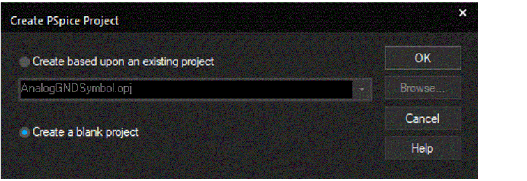
-
Click OK.
Thetutorialproject is created. In the project manager window, a design file,tutorial.dsnis created. Below the design file, a schematic folder with the nameSCHEMATIC1is created. The folder has a schematic page namedPAGE1.
Figure 2-2 Project Manager window .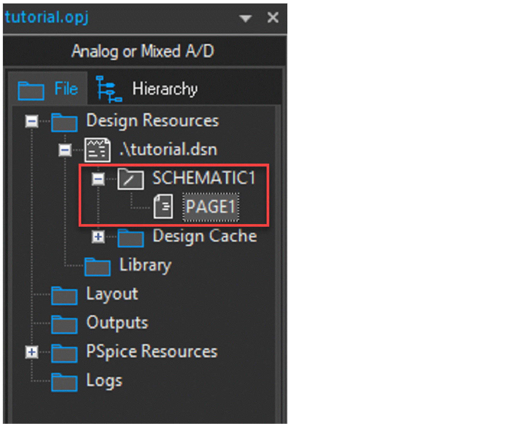
Creating a Design
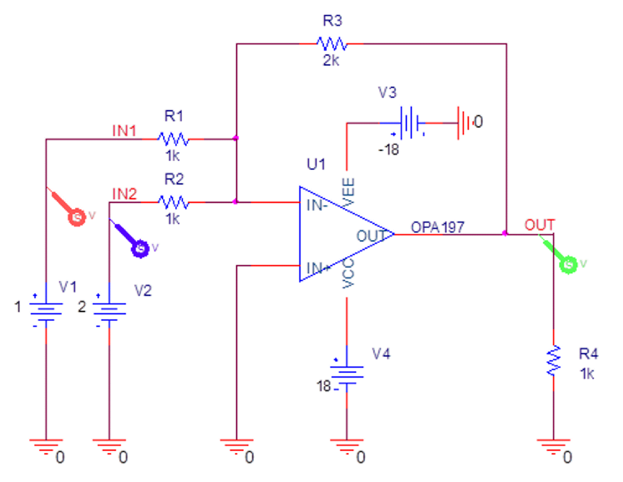
You will now create the design of the Inverting Summing Amplifier as shown in the following figure.
Figure 2-3 Schematic design for the inverting summing amplifier
You will also perform the following tasks in order to create the schematic design as shown above:
- Placing the Op-Amp
- Placing DC Voltage Sources using Modeling Application
- Placing Ground Symbols
- Placing the Resistors
- Connecting the Components
- Assigning Net Aliases
- Placing Markers
Placing the Op-Amp
To place OPA197, do the following:
-
Select Place – PSpice Component – Search or click the Launch PSpice Part Search icon (
 ) on PSpice toolbar.
The PSpice Part Search window opens.Figure 2-4 PSpice Part Search window
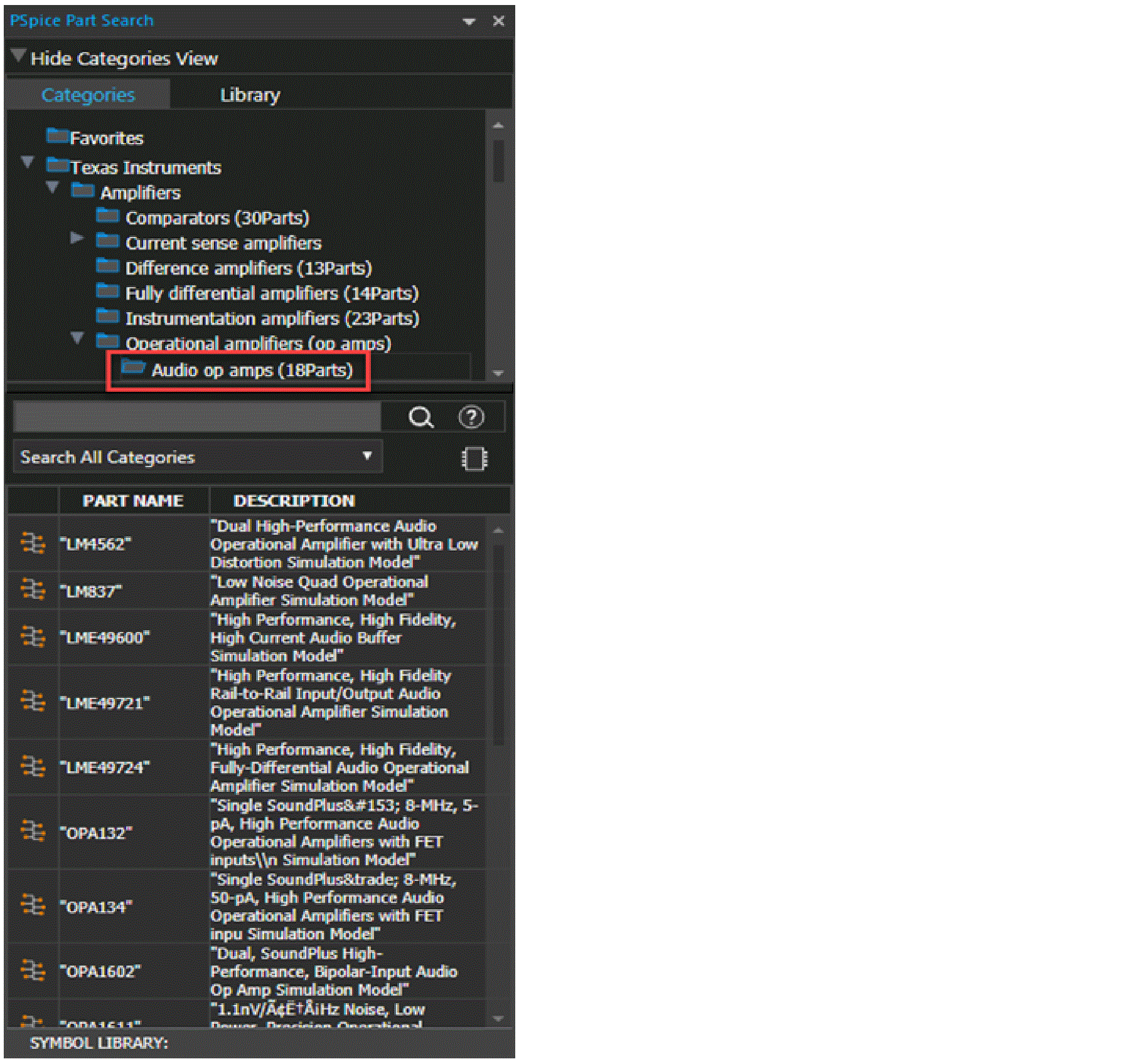
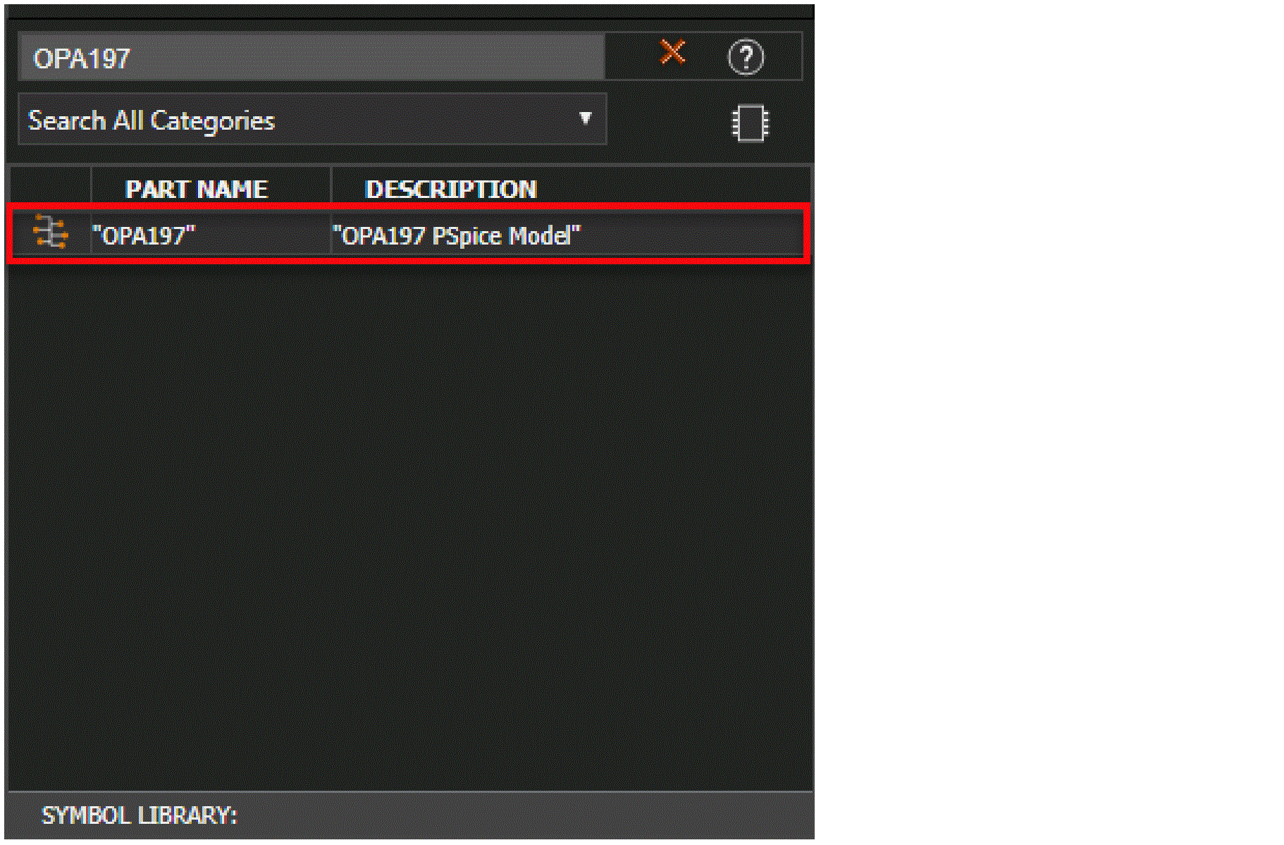
-
Search for OPA197 in the part search field, and click
 icon.
icon.
OPA197 appears in the search result. -
Double-click OPA197 and click the schematic page to place the part.
- Right-click and select End Mode or press Esc.
Placing DC Voltage Sources using Modeling Application
-
Select Place – PSpice Component – Modeling Application or click the Launch Modeling Application icon (
 ) on the PSpice toolbar.
The Modeling Application pane opens. -
Select Sources – Independent Sources.
Figure 2-5 Modeling Application window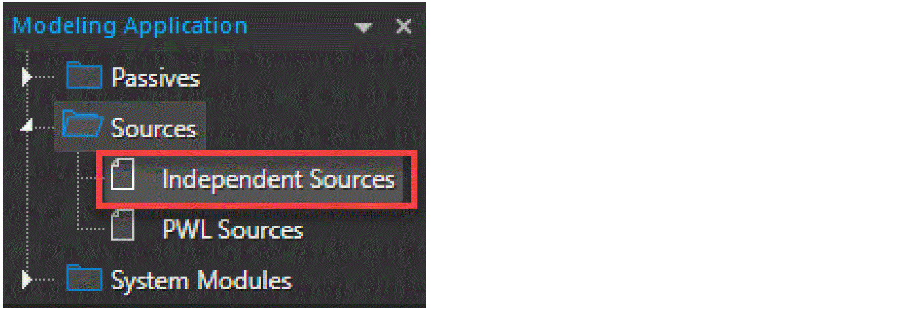
- Click DC.
- Select Voltage and Ideal DC.
-
Select DC Voltage as
1and click Place to place the voltage source.
Figure 2-6 Independent Sources windowFigure 2-7 Voltage V1 on the schematic page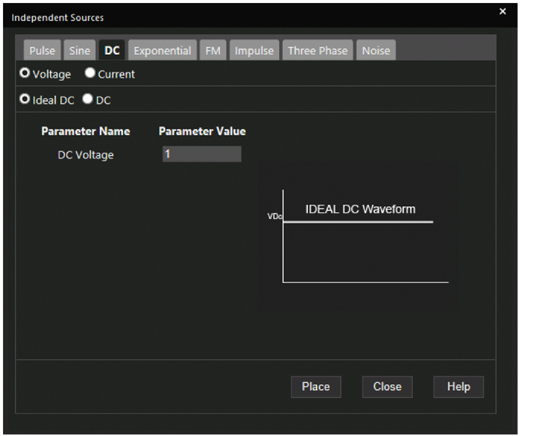
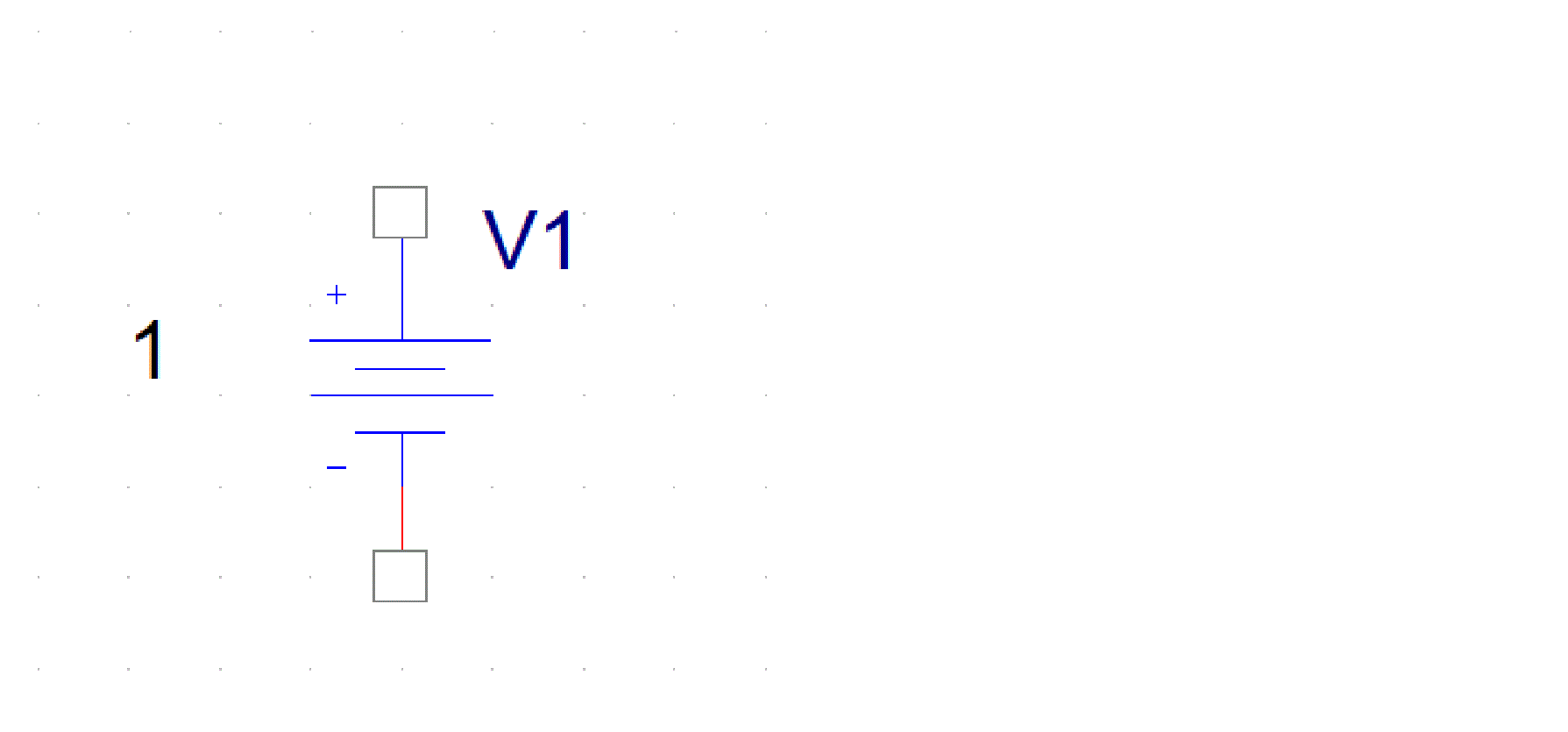
-
Similarly, place 3 more DC voltage sources with the following voltage values:
Voltage Name Voltage Value - To save the design, select File – Save or press CTRL+S.
Placing Ground Symbols
- Select Place – PSpice Component – PSpice Ground.
- Click the schematic page to place the part.
- Right-click and select End Mode or press Esc.
Placing the Resistors
-
Select Place – PSpice Component – Resistor.
The part symbol is attached to a pointer. - Click the schematic page to place the resistor.
- To stop placing the resistor, right-click and select End Mode or press Esc.
-
To change the value, double-click the value of the resistor.
The Display Properties window opens.
Figure 2-8 Display Properties windowFigure 2-9 Resistance R1 on the schematic page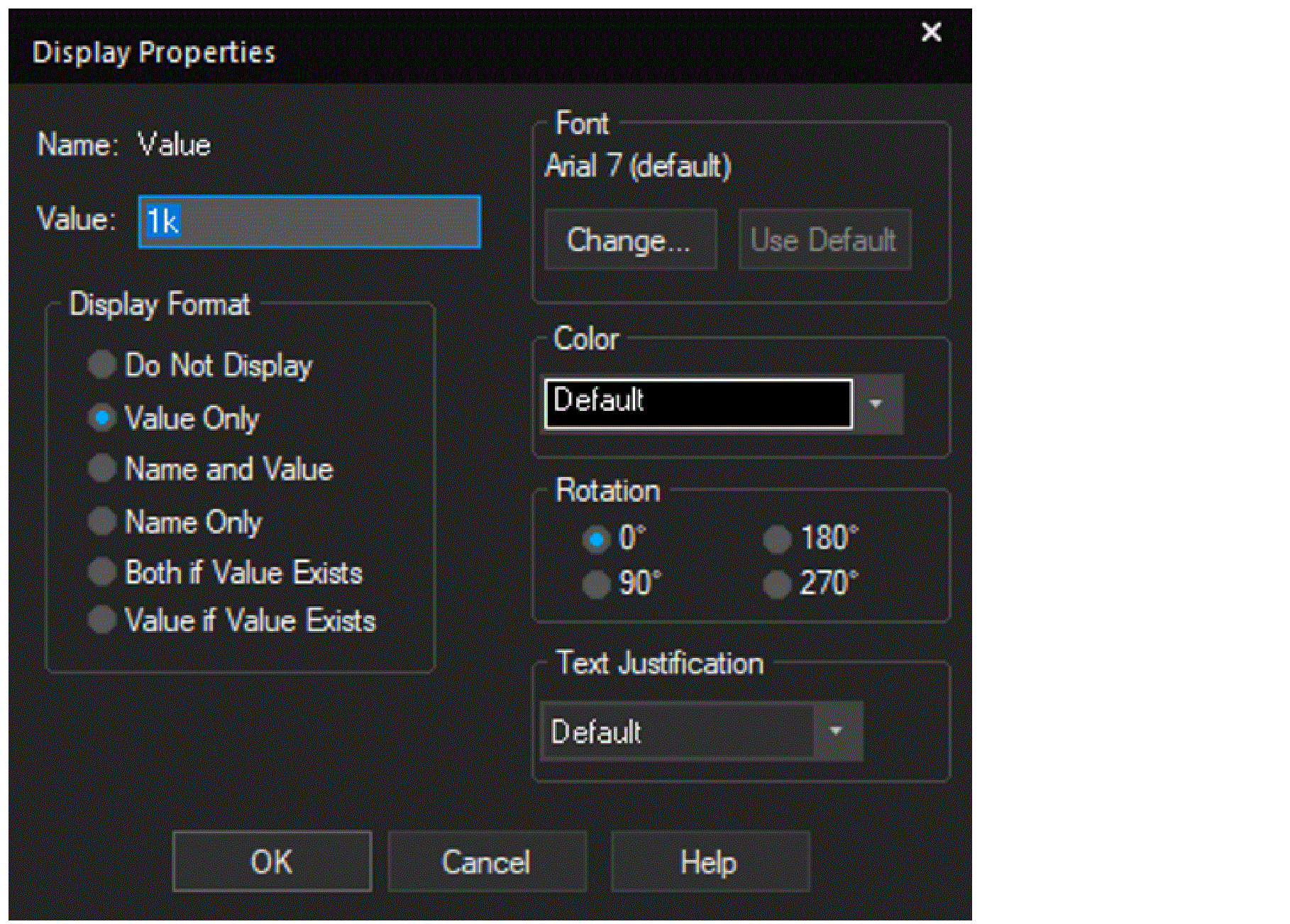
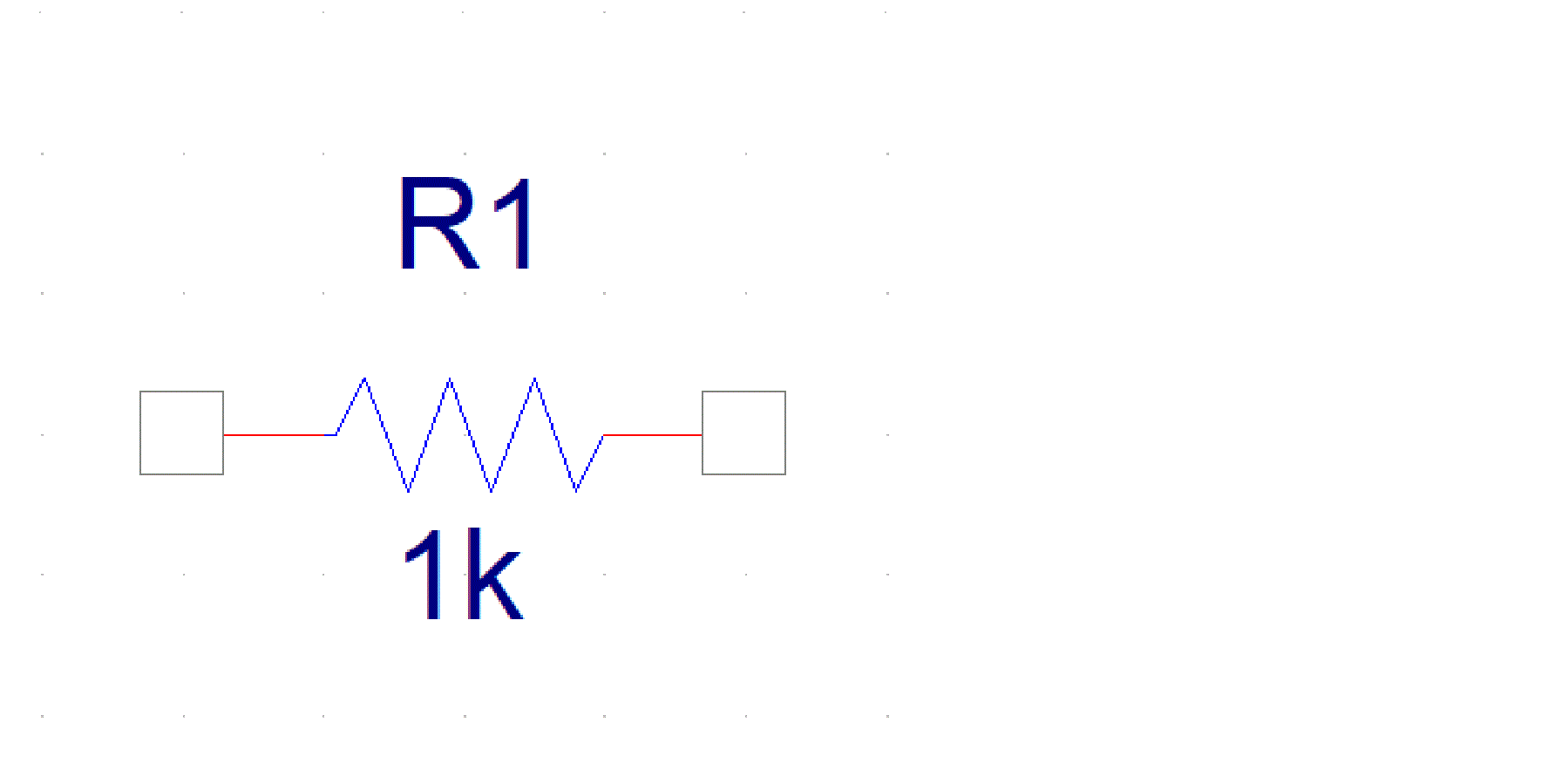
-
Similarly, place 3 more resistances, and specify the value shown in the following figure.
Resistance Name Resistance Value - Click OK.
Connecting the Components
-
Select Place – Wire, press W, or click the Place wire icon (
 ) on the Draw Electrical toolbar.
The pointer changes to a crosshair. - Click any valid connection point to end the wire.
Assigning Net Aliases
A net is not required to have an alias, but by using an alias, you can establish connectivity. To create a net alias, do the following;
-
Select Place - Net Alias.
The Place Net Alias dialog opens. -
Enter the net alias text in the Alias dialog box and click OK.
Figure 2-10 Place Net Alias windowA rectangle representing the net alias is attached to the pointer.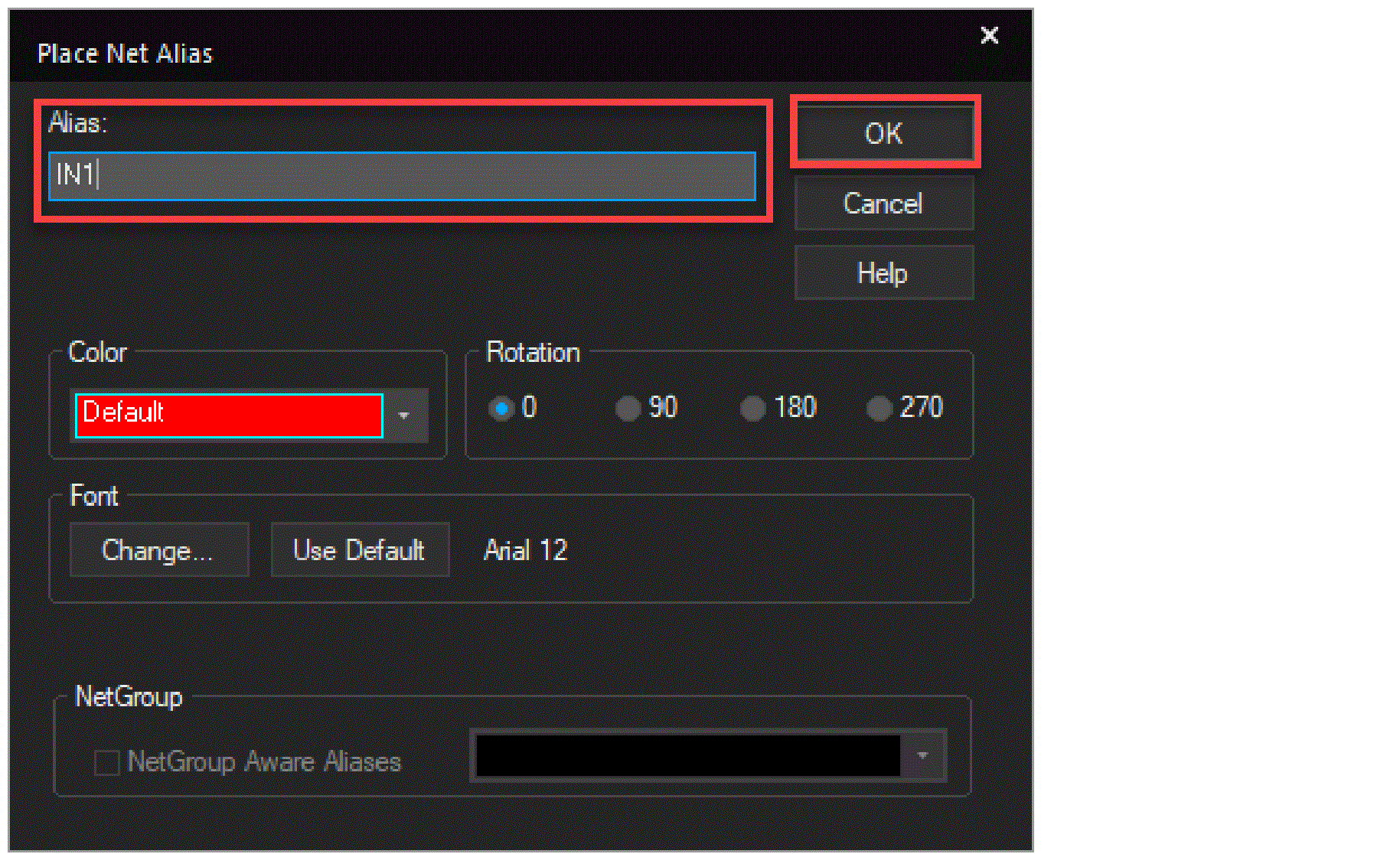
-
Use the mouse to move the net alias and click the left mouse button on the wire to place the net alias.
The net alias appears in the selection color.
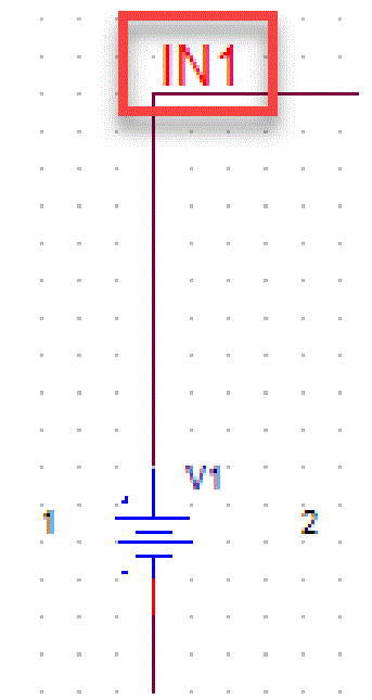
-
Similarly, place the net aliases
IN2andOUT. - Press Esc to dismiss the net alias tool.
Creating a New Simulation Profile
-
Select PSpice – New Simulation Profile or click the New Simulation Profile icon (
 ) on the PSpice toolbar.
The New Simulation dialog box opens -
Specify the name of the new simulation profile as
TRAN. -
In the Inherit From drop-down list, ensure that
noneis selected and click Create.
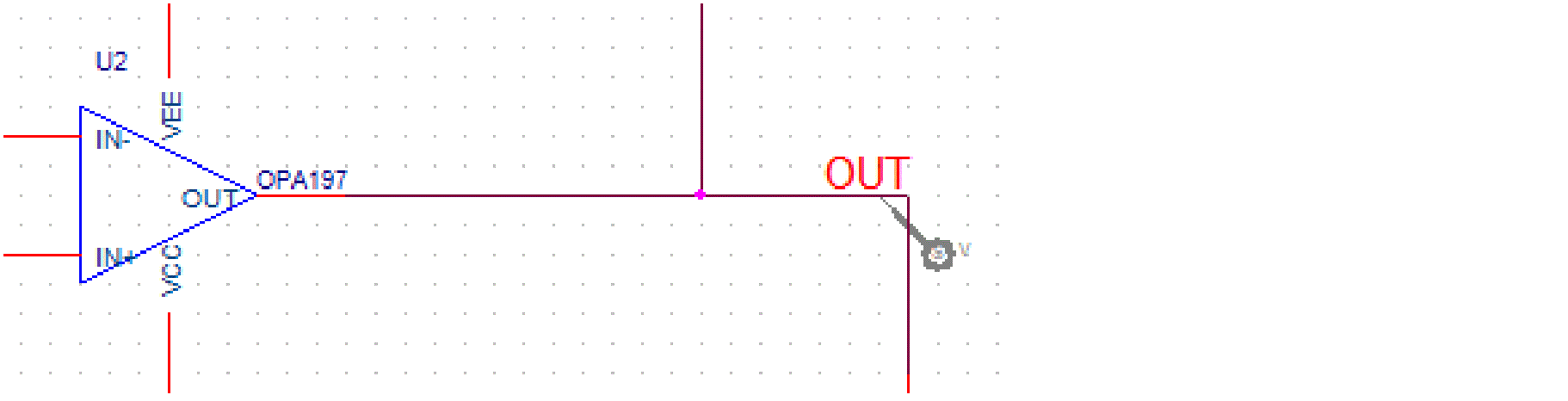
Figure 2-11 New Simulation windowThe Simulation Setting dialog box appears with the Analysis tab selected.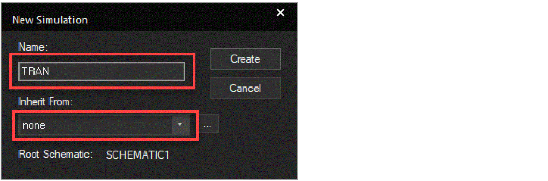
Figure 2-12 Simulation Settings - Analysis tab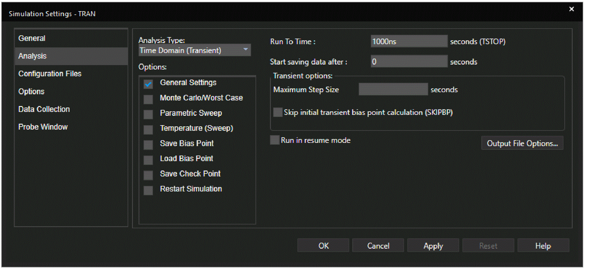
- Retain all the default settings and click OK to close the dialog box.
Placing Markers
To visualize the circuit behavior and determine the validity of your circuit design, you can plot the output waveforms in the Probe window. By analyzing the output waveforms, you can evaluate your circuit for performance.
For PSpice for TI to display output waveforms in the Probe window, you need to place markers in your circuit design in Capture to indicate the points where you want to see simulation waveforms displayed in PSpice for TI.
- before simulation to limit results written to the waveform data file, and automatically display those traces in the active Probe window.
- during or after simulation, to automatically display traces in the active Probe window.
You will now add Voltage markers to view the output waveforms in the Probe window. To do so:
-
Select PSpice – Markers – Voltage Level or click the Voltage/Level Marker icon (
 ) on the PSpice toolbar.
 -
Place the first marker at the 1 Volt power supply V1.
-
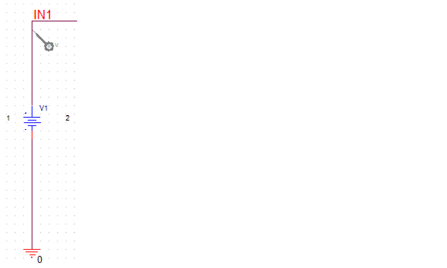
Place the second marker at the 2 Volt power supply V2.
-
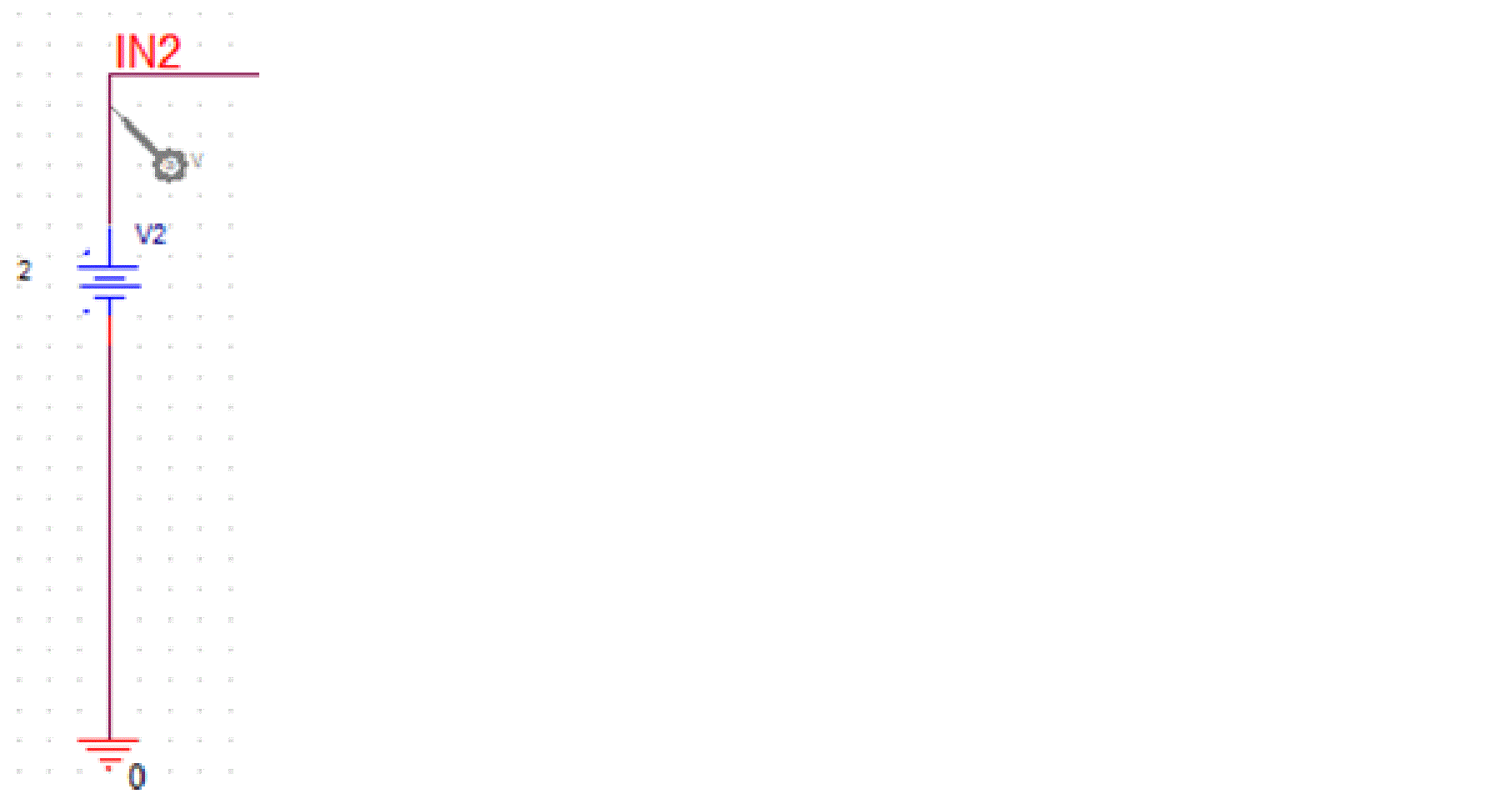
Place the third marker at the output of the op-amp.
Running the simulation
To simulate the design, choose PSpice – Run or click the Run PSpice icon (![]() ) on the PSpice toolbar.
) on the PSpice toolbar.
The plot window opens with simulation result.
Figure 2-13 Output Waveform - Probe window
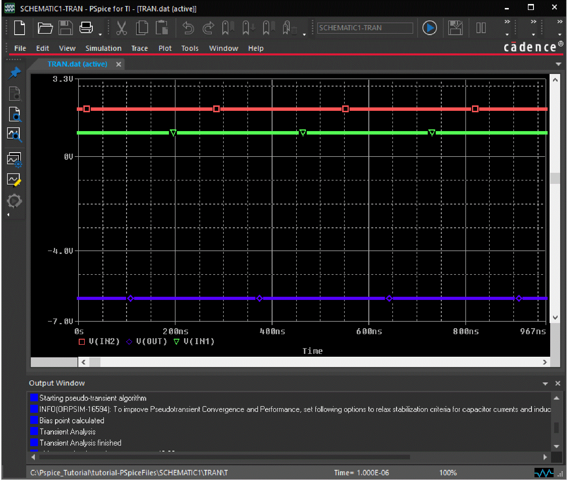
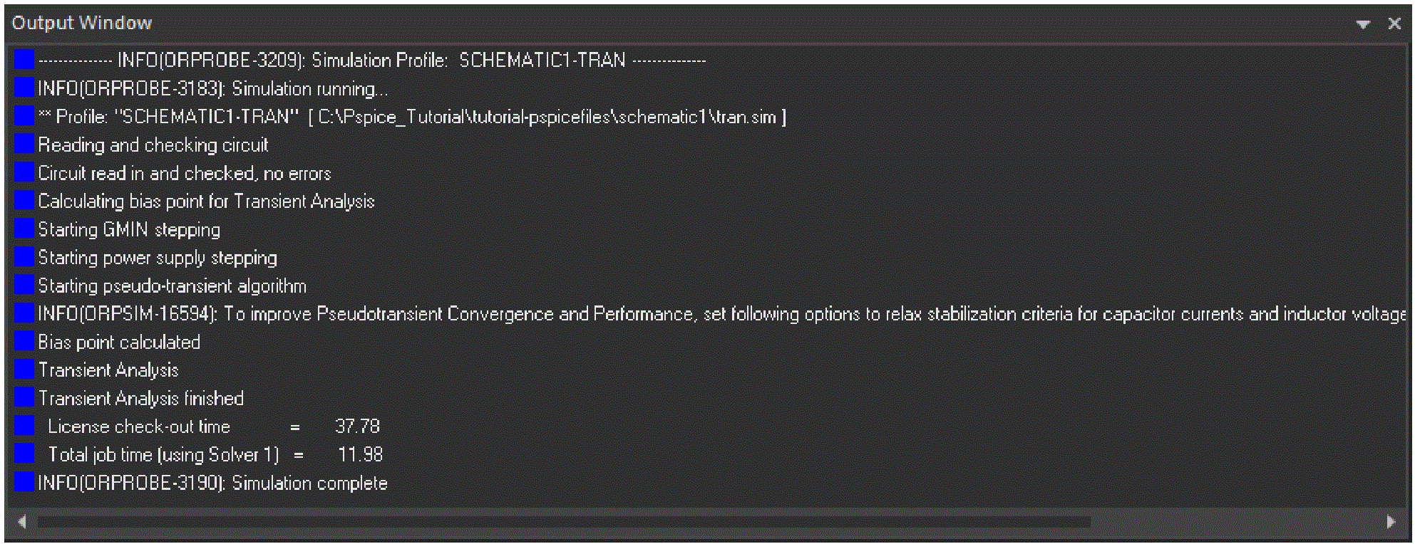
By default, you will see the output window as shown in the following figure with simulation complete status:
To view the probe cursor window, select View – Cursor Window or click the Toggle Cursor icon (![]() ) on the Probe Window toolbar.
) on the Probe Window toolbar.
The Probe Cursor window opens.
Figure 2-15 Probe Cursor window
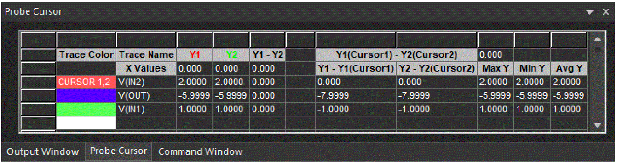
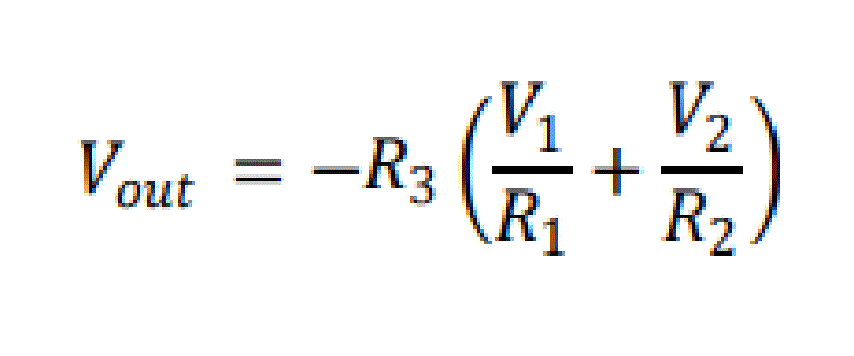
The Probe Cursor window shows the value of the output voltage corresponding to the values of the input voltages and resistances according to the formula of the inverting summing amplifier:
Return to top