| Xilinx has offered low cost ASIC versions of our FPGAs since 1990,
providing the benefits of both flexible logic development and easy-to-use
cost reduction for high volume designs. By mapping the SRAM-based programmable
elements in our FPGAs to an efficient gate array architecture, we can deliver
a lower cost device that closely matches the functionality of the XC4000
FPGA. |

|
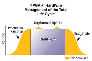
HardWire Arrays, along with Xilinx FPGAs, provide a complete logic development
solution. You get fast and efficient prototyping for system
development, plus as low cost, high volume production capability. Xilinx
FPGAs and HardWire Arrays are interchangeable, offering flexibility for
cost reductions, future design changes, and end-of-life management of your
product.
Xilinx HardWire Array Features
-
The only turn-key, low risk conversion path for Xilinx FPGAs
-
Patented DesignLock conversion methodology
-
Requires minimal customer engineering resources
-
Supports conversion of all Xilinx FPGA features, including:
-
Select-RAM
-
JTAG with Global Buffers
-
Configuration Emulation
-
Power on Reset (POR)
-
Speeds up to 1
-
Packages up to PQ240 and BG352
Xilinx HardWire Arrays consist of pin-compatible mask programmed versions
of Xilinx FPGAs. The XH3 Series is used for conversion of the XC4000E
and XC4000EX FPGA families. We convert XC4000XL FPGAs into XC4400XL HardWire
Arrays.
|
FPGA
|
HardWire Equivalent
|
|
XC4000E, XC400EX
|
XH3
|
|
XC4000XL
|
XC4400XL
|
We use the routed, verified FPGA database files to generate a HardWire
device that is functionally compatible with the FPGA; all of the logic
developed in the FPGA design is preserved. The smaller ASIC die reduces
the cost of the device.
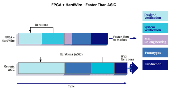
In generic ASIC development, design verification,
and timing simulation must be completed before prototypes are manufactured.
Only then can system verification take place with working silicon.
With the Xilinx HardWire Array development flow, you will have working
devices starting the first day of design. This flexibility accelerates
system verification and product development.
With Xilinx HardWire Arrays, there is no logic
to re-work, no simulation to re-run, no test vectors to write, and no changes
to your PCB layout. Qualification is simple, because HardWire prototypes
come in the same package and pin-out as the FPGA, and are tested on the
same PC board. No other FPGA conversion path can offer you the same
benefits with such low risk and minimal effort.
Easy Conversion Process
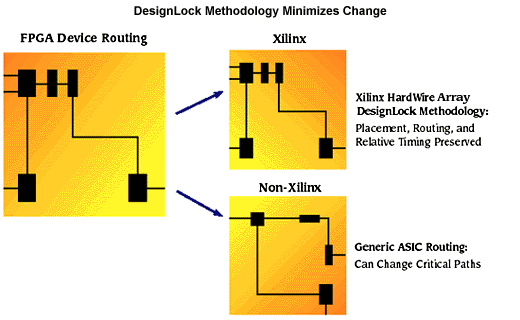
Converting from a Xilinx FPGA to a HardWire Array
is simple. You submit the completed FPGA design files to Xilinx for a quick
design check. Our in-house HardWire Design Center then converts the design
using our patented DesignLock conversion methodology. In the DesignLock
process, each FPGA Configurable Logic Block (CLB) is mapped to the HardWire
device in the same relative position. All timing, placement, and routing
contained in the tested and verified FPGA design files are preserved. This
simple process reduces the time required to cost-reduce an FPGA design
while maintaining all of the functionality.
We use a patented Universal Configuration Emulation
megafunction (UCE) to reproduce any Xilinxsupported configuration mode.
A similar Universal I/O function (UIO) is also implemented in each device
to act as a fully compatible I/O controller. The UCE and UIO functions
reduce both functional mismatches and design conversion time.
Our Design Center experts are Xilinx FPGA conversion
specialists who have converted over 900 customer designs. No other
company has more experience converting Xilinx FPGAs
HardWire Array Conversion
| Features |
Benefits |
| Turn-key design conversion flow. |
All logic and nets preserved |
| Mapping preserves FPGA timing relationships |
No customer functional simulation.
No timing simulation required. |
| Full Scan insertion |
No customer test vectors required |
| Universal Configuration Emulation and I/O Macros. |
Reduced conversion time. Assured prototype success. |
| Pin-out and package compatibility |
Similar package as FPGA.
No package re-qualification or board re-layout required. |
Test Vectors
System designers have found that achieving high fault coverage by generating
test vectors can be a time consuming, expensive task, especially for high
density, high function logic designs. The Xilinx HardWire conversion
process uses full scan logic and Automatic Test Pattern Generation software
to develop test vectors. The design engineer does not have to spend
time writing vectors and submitting them to Xilinx.
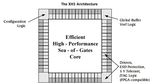
Xilinx XH3 FPGA-Specific HardWire Arrays
The XH3 HardWire Arrays are unique because they include key Xilinx
FPGA features built into the die. The XH3 is manufactured in 0.5
micron process for XC4000E and XC4000EX conversions. The XH3 Series
features a dense sea-of-gates architecture that optimizes both logic and
routing capability by using highly tuned drive and logic cells. XH3 Series
devices contain key global buffers, power-on-reset (POR) circuitry, and
configuration control built into the corners of the die. The JTAG ring
is also built into the I/O ring on the silicon. These architectural
advances provide the closest possible match with the FPGA features while
minimizing conversion time.
XH3 0.5 Micron Product Family for XC4000E/EX
Part
Number |
Maximum Usable
Gates |
Pads
Available |
| XH302 |
14000 |
112 |
| XH304 |
28000 |
172 |
| XH306 |
42000 |
204 |
| XH308 |
62000 |
240 |
| XH310 |
97000 |
292 |
| XH312 |
146000 |
352 |
XC4000XL FPGA Conversions
Xilinx converts XC4000XL FPGAs into our 0.45 micron XC4400XL HardWire
Arrays. We use the same DesignLock conversion and test vector generation
processes described above to convert all of the logic in the FPGA design
into a multi-mask gate array. All the FPGA features used in the FPGA design
are also converted into the HardWire Array. The XC4400XL is interchangeable
with the FPGA, and is cost-effective device for high-volume applications.
The Make vs. Buy Decision
Customers encounter a Make Versus Buy decision when they consider
how to develop their systems. Compare the simple, low risk Buy approach
of using Xilinx FPGAs and HardWire Arrays with the greater effort and higher
risk of using a traditional ASIC development flow (the Make decision).
| Turn-Key
Approach |
|
Non
Turn-Key Approach |
|
| HardWire Array |
|
Customer |
|
Customer |
|
ASIC Vendor |
| |
|
Design entry/
system verification |
|
Design entry
|
|
|
|
Design review
Design conversion
|
|
|
|
|
|
Design review &
retarget |
| |
|
|
|
Design verification
Fix design errors
|
|
|
|
Place and route
|
|
|
|
|
|
Place and route
|
Generate timing
report |
|
Review timing
report |
|
Timing simulation
Fix timing errors
Write test vectors
|
|
|
|
Build prototypes
|
|
|
|
|
|
Build prototypes
|
| |
|
Test prototypes
|
|
Test prototypes
System verification
|
|
|
Build production
units |
|
|
|
As-needed:
logic redesign &
prototype |
|
Build production
units |
ASIC vendors manufacture the device, but you take on the effort of ensuring
the design was re-targeted correctly in the vendors libraries. Furthermore,
you are responsible for verifying the silicon implementation works in the
system. Any problems throughout the design process are your responsibility
to fix.
That is not true with Xilinx HardWire Arrays. With this option,
you buy proven, off-the-shelf Xilinx FPGAs to get the fastest time to market
and the most flexible production solution. When higher production
volumes require a lower cost, you can use the Xilinx turn-key HardWire
conversion process. Xilinx takes the responsibility of converting
the FPGA design to a cost-effective HardWire Array by using a unique, made-for-FPGA
conversion flow.
The Xilinx Buy approach lets you focus your engineers on where your
company adds value. Only Xilinx offers this complete solution. |