Instructions
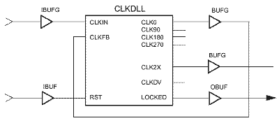
The circuit shown below implements a 2x clock multiplier and also
uses the CLK0 clock output with zero ns skew between registers on
the same chip. A clock divider circuit could alternatively be implemented
using similar connections. Because any single DLL can only access
at most two BUFGs, any additional output clock signals must be routed
from the DLL in this example on the high speed backbone routing.
VHDL
library ieee;
use ieee.std_logic_1164.all;
library unisim;
use unisim.vcomponents.all;
entity dll_standard is
port (CLKIN : in std_logic;
RESET : in std_logic;
CLK0 : out std_logic;
CLK2X : out std_logic;
LOCKED: out std_logic);
end dll_standard;
architecture structural of dll_standard is
signal CLKIN_w, RESET_w, CLK0_dll, CLK0_g, CLK2X_dll, LOCKED_dll :
std_logic;
begin
clkpad : IBUFG port map (I=>CLKIN, O=>CLKIN_w);
rstpad : IBUF port map (I=>RESET, O=>RESET_w);
dll : CLKDLL port map (CLKIN=>CLKIN_w, CLKFB=>CLK0_g, RST=>RESET_w,
CLK0=>CLK0_dll, CLK90=>open, CLK180=>open, CLK270=>open, CLK2X=>CLK2X_dll,
CLKDV=>open, LOCKED=>LOCKED_dll);
clkg : BUFG port map (I=>CLK0_dll, O=>CLK0_g);
clk2xg : BUFG port map (I=>CLK2X_dll, O=>CLK2X);
lckpad : OBUF port map (I=>LOCKED_dll, O=>LOCKED);
CLK0 <= CLK0_g;
end structural;
Verilog
// XAPP174
//
// DLL 1X and 2X Example
//
module dll_standard (CLKIN, RESET, CLK0, CLK2X, LOCKED);
input CLKIN, RESET;
output CLK0, CLK2X, LOCKED;
wire CLKIN_w, RESET_w, CLK0_dll, CLK2X_dll, LOCKED_dll;
IBUFG clkpad (.I(CLKIN), .O(CLKIN_w));
IBUF rstpad (.I(RESET), .O(RESET_w));
CLKDLL dll (.CLKIN(CLKIN_w), .CLKFB(CLK0), .RST(RESET_w), .CLK0(CLK0_dll),
.CLK90(), .CLK180(), .CLK270(), .CLK2X(CLK2X_dll), .CLKDV(), .LOCKED(LOCKED_dll));
BUFG clkg (.I(CLK0_dll), .O(CLK0));
BUFG clk2xg (.I(CLK2X_dll), .O(CLK2X));
OBUF lckpad (.I(LOCKED_dll), .O(LOCKED));
endmodule
|