| |
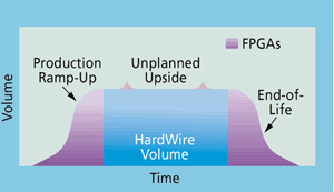
The Xilinx HardWire FpgASIC capability is part of a complete solution for high volume applications. You get fast, efficient prototyping, system development, and initial production using our FPGAs and you also get low cost, high volume production capability using our FpgASICs. Our FPGAs and FpgASICs are interchangeable, offering you flexibility for cost reductions, future design changes, and end of life maintenance of your systems. HardWire FpgASIC is a category of mask-programmed gate arrays. The same design files used to create the original FPGA are used throughout the FpgASIC conversion process; both the placement and routing of the original FPGA are preserved. By mapping the SRAM-based programmable elements in our FPGAs to a very efficient gate array architecture, we can deliver a highly competitive, state of the art ASIC that matches your FPGA design. FPGA+HardWire FpgASIC management of the total life cycle
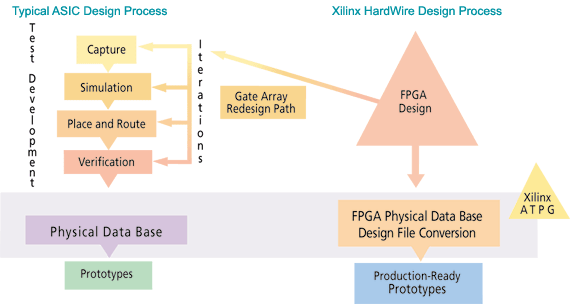
We have offered low cost ASIC versions of our FPGAs since 1991, allowing you to enjoy the ease of use and time to market benefits of FPGAs, and still reduce the cost of your high volume designs. The path from design to high volume production, using Xilinx FPGAs and FpgASICs, is much faster and easier, with less risk and less cost, than any other method. Converting from a Xilinx FPGA to a HardWire FpgASIC is simple. Your completed FPGA design files are submitted to Xilinx for a thorough design check. We then convert the design using our patented DesignLock™ conversion methodology, which maps each FPGA Configurable Logic Block (CLB) to the HardWire device in the same relative position. The placement and routing contained in your tested and verified FPGA design files are preserved. Our in house design center experts are Xilinx conversion specialists who have converted over 1,000 customer designs. No other company has more experience converting Xilinx FPGA designs.
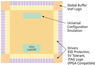
The XC4400 FpgASIC uses a multi-mask process for XC4000E conversions. These HardWire FpgASICs support all of the features of each FPGA and take advantage of our advanced submicron processes to offer cost effective solutions for high-volume production. The XH3 FpgASIC family contains critical FPGA features built into the base silicon of the gate array. Because of this, we can achieve a smooth, error free cost reduction for XC4000E and XC4000EX devices.
|
||||||||||||||||||||||||||||||||||||||||||||||||||||||||
| | Product Overview Cover | Corporate Overview | Virtex-Redefining the FPGA | | CPLDs - A New Generation | FPGAs - A Heritage of Excellence | Hardwire FpgASICs | Software Solutions | | Core Solutions | High-Reliability Products | Technical Service and Support | |
||||||||||||||||||||||||||||||||||||||||||||||||||||||||