| |
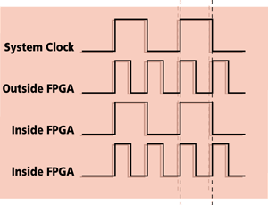
Fully Digital Delay Locked Loops (DLL)
With an available density range up to 1,000,000 gates, the Virtex series allows unprecedented system level integration, supported by a highly efficient segmented routing structure which provides abundant routing resources and assures consistent performance.
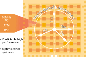
SmartIP™ Optimized Vector-Based Interconnect
Data intensive applications require high-bandwidth memory. The Virtex SelectRAM+ memory hierarchy provides high bandwidth for memory block sizes in bytes (distributed memory), kilobytes (block memory), and megabytes (SSTL3 interface to external DRAM and SRAM). |
||||||||||||||||||
| | Product Overview Cover | Corporate Overview | Virtex-Redefining the FPGA | | CPLDs - A New Generation | FPGAs - A Heritage of Excellence | Hardwire FpgASICs | Software Solutions | | Core Solutions | High-Reliability Products | Technical Service and Support | |
||||||||||||||||||