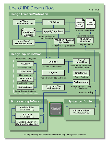
Plan out your design and enter it as either HDL (VHDL or Verilog), structural schematic, or mixed-mode (schematic and RTL).
After you have defined your design, you must verify that it functions the way you intended. After creating a testbench using WaveFormer Lite, use the ModelSim VHDL or Verilog simulator to perform functional simulation on your schematic or HDL design.
A design must be synthesized if the design was created using VHDL or Verilog. Use Synplify AE or Synplify Pro from Synplicity to generate your EDIF netlist. You can re-verify your design "post-synthesis" using the VHDL or Verilog ModelSim simulator used in step two.
While all RTL code must be synthesized, pure schematic designs are automatically "netlisted" out via the Libero tools to create a structural VHDL or structural Verilog netlist.
After you have functionally verified that your design works, the next step is to implement the design using the Actel Designer software. The Designer software automatically places and routes the design and returns timing information. Use the tools that come with Designer to further optimize your design. Use Timer to perform static timing analysis on your design, ChipEditor or ChipPlanner to customize your I/O macro placement, PinEditor for I/O customization, SmartPower for power analysis, and NetlistViewer to view your netlist.
After you are done with design implementation, you can verify that your design meets timing specifications. After creating a test bench using WaveFormer Lite, use the ModelSim VHDL or Verilog simulator to perform timing simulation.
Once you have completed your design, and you are satisfied with the timing simulation, create your programming file. Depending upon your device family, you need to generate a Fuse, Bitstream, or STAPL programming file.
